TI has a lot of "dedicated headphone ICs". Every big Cell Phone manufacturer is in a position to demand some customization.
Until now my preferred GP headphone amp is the TPA6130A2 and the TPA6133A2 I pushed them to make (it doesn't need a uP to start it). They also have the TPA6120A2 (a repurposed DSL driver) that also has outstanding performance. There are a few others in the family as well, depending on your goals.
The target of the OPA6122 judging from the footprint, power requirements etc, is the new wave of cell phones with high resolution audio ambitions. A design win is a minimum of 1 million chips usually. Its hard to make fewer phones than that. Both AKM and ESS have new high performance DAC chips targeted at these opportunities as well. ESS has a new headphone amp chip they are promoting with over the top claims as well. We all are the beneficiaries of this market.
I have a couple of questions for John Caldwell please -
John, there's no doubt that the OPA1622 is an outstanding op-amp for headphone applications, especially for lower impedance phones, but how do you think it would rate sonically against say the TPA6120a2 or a low distortion audio op-amp + buffer in the op-amp's feedback loop arrangement if only 300-600 Ohm phones are used? Would the lower distortion really make an audible difference?
Another thought - is there any point trying to uses a CCS to bias the output stage further into Class A as with conventional op-amps or would that screw up your special output stage fix? If it is worth it, could you suggest a value for the bias current?
Last edited:
I have a couple of questions for John Caldwell please -
John, there's no doubt that the OPA1622 is an outstanding op-amp for headphone applications, especially for lower impedance phones, but how do you think it would rate sonically against say the TPA6120a2 or a low distortion audio op-amp + buffer in the op-amp's feedback loop arrangement if only 300-600 Ohm phones are used? Would the lower distortion really make an audible difference?
Another thought - is there any point trying to uses a CCS to bias the output stage further into Class A as with conventional op-amps or would that screw up your special output stage fix? If it is worth it, could you suggest a value for the bias current?
Those loads don't really require the high output current capabilities of the OPA1622 (or the TPA6120A2 or output buffer products, e.g. BUF634). The OPA1622 will still show exceptional performance in those applications, but I think the debate of whether it is "necessary" becomes more difficult because there are a number of op amps which can maintain very low distortion with a 600 ohm load. I guess your question is really which internal amplifier topology sounds better in the absence of extraordinary demands for output current?
Biasing old op amps into Class A made a lot of sense. Most of them were on processes that only had lateral PNP devices, and so the output stages tended to be quasi complementary types with poor symmetry. I'm not convinced yet that biasing the OPA1622 output stage into Class A provides major sonic advantages. Even crossover distortion is limited on the device because of the biasing scheme employed on the output transistors. I show a plot of the output stage gain vs. output voltage here: Amp up your cans: Distortion in headphone amplifiers (Part 4) - Precision Hub - Blogs - TI E2E Community
If you want to try it, give it a shot! I'd love to hear your observations as to whether the sound was improved. It's not going to screw up the output stage at all, it'll just use half of it
")
The sonic advantages in my experience come primarily from having a cleaner supply when biased into class A. How's the PSRR of the OPA1622 into a representative load when displaced from the zero point?
PSRR would only vary if the open loop gain of the amplifier significantly varied with output voltage. As long as the output isn't clipping, the open loop gain spec (136 dB typical, 600 ohm load) is valid regardless of which output device is conducting current. So PSRR of the amplifier is unchanged, but you make a good point that the waveform imposed on the supplies will be a sinusoid rather than a half-wave rectified sine.
Last edited:
Admittedly I did the simulation with the normal bipolar transistor models (LTspice) in the output stage, but I found that the PSRR of the output stage by itself varied with load and with the output current. It looked very good indeed with no output load connected and with its output mid-rails.
Admittedly I did the simulation with the normal bipolar transistor models (LTspice) in the output stage, but I found that the PSRR of the output stage by itself varied with load and with the output current. It looked very good indeed with no output load connected and with its output mid-rails.
What was the output stage topology? I would guess it was a classic emitter-follower type? In this case I wouldn't be surprised at all that the PSRR of the output stage itself would vary with load impedance, because the local feedback in the output stage depends on the load impedance. Also, matching between the Early voltages of the two output transistors would seem to cause some variation in PSRR of the output stage with output voltage. Did you look at a CFP output stage at all?
Yes it was the EF2 topology, fairly standard. I didn't play with CFP but had a look at the diamond buffer which seemed to have a small (about 6dB) PSRR advantage over EF2.
I looked at your DS and your output swings impressively close to the rails - so does that mean you're not using EF but something more efficient in rail voltage utilization?
So back to our earlier discussion, given that the PSRR of the output stage (assuming EF) varies over output current and load impedance, wouldn't the closed loop PSRR also vary in the same manner, just reduced by the loop gain? Or am I missing something vital here?
The OPA1622 does not use an EF output stage, that's correct.
I will grant that it's possible for PSRR to vary due to the PSRR of the output stage, but there are a lot of variables to consider:
1. Output stage topology
2. Is there a local miller loop around the output stage?
3. Output transistor biasing scheme. My gut says a Monticelli biasing scheme, which is very popular in modern op amps and essentially treats the non-conducting output transistor like a constant current source, would be more resistant to variations.
4. Output transistor parameters: Early voltage and bias point of course, since the transistor output impedance is really what we're talking about. Also Cob which might couple PS noise to the base in an EF topology.
I still believe that variations in the output stage PSRR are going to be significantly smaller than the dominant sources of PSRR degradation such as compensation capacitors tied directly to the supply rails, and mismatched parasitics to the substrate which likely do not depend on the loading. The end result being that if you want to isolate the supply ripple to one of the rails through class A biasing, pick the one that the amplifier is better at rejecting (even at minimal loading). In the OPA1622's case that would suggest the positive supply rail. Cool discussion!
Or bootstrap the entire opamp at the board level. Attach 2SD882/2SB772 emitter followers and level shifters which set
Now the output transistors work at constant VCE (Vsupply - Vout = constant!) so their Early effect is unimportant. Mismatched parasitics to the substrate are also unimportant since the substrate moves in perfect sync with the output. Common mode effects are eliminated too.
- Opamp PlusSupply = +15VDC + (K * Vout)
- Opamp MinusSupply = -15VDC + (K * Vout)
Now the output transistors work at constant VCE (Vsupply - Vout = constant!) so their Early effect is unimportant. Mismatched parasitics to the substrate are also unimportant since the substrate moves in perfect sync with the output. Common mode effects are eliminated too.
Or bootstrap the entire opamp at the board level. Attach 2SD882/2SB772 emitter followers and level shifters which setWhere K is a constant somewhere between 0.950 and 1.000
- Opamp PlusSupply = +15VDC + (K * Vout)
- Opamp MinusSupply = -15VDC + (K * Vout)
Now the output transistors work at constant VCE (Vsupply - Vout = constant!) so their Early effect is unimportant. Mismatched parasitics to the substrate are also unimportant since the substrate moves in perfect sync with the output. Common mode effects are eliminated too.
Great points Mark, just watch out for weird behavior on power up and power down!
To add to my previous post, many op amps also cascode their output devices (very common in CMOS) which of course would improve output stage PSRR. Bob Cordell has a brief section on this in his power amplifier book.
John,
I wouldn't much worry about Abrax's comments about rail pumping and PSRR hand wringing. It's his schtick with any/every opamp under/around the sun, and yet, he's been peculiarly reticent with data showing this effect (scope traces/distortion plots/FFT's/something!), much less its magnitude. On older devices with much lower loop gain, PSRR, and nonlinear OPS driven to their limits, he probably has a point, but that's not the case here (also assuming following the datasheet wrt local decoupling/layout).
I wouldn't much worry about Abrax's comments about rail pumping and PSRR hand wringing. It's his schtick with any/every opamp under/around the sun, and yet, he's been peculiarly reticent with data showing this effect (scope traces/distortion plots/FFT's/something!), much less its magnitude. On older devices with much lower loop gain, PSRR, and nonlinear OPS driven to their limits, he probably has a point, but that's not the case here (also assuming following the datasheet wrt local decoupling/layout).
Abrax -- I tried to provide some context as to your posting history on this particular subject, which is, honestly, relevant to the ongoing discussion. Such context may steer it away from pet theories tested out on every new opamp. Simply put, figures such as 18 and 57-59 would bear out your concerns; so, if the effect is there, it's well suppressed. If you want to earnestly dig into your concerns, it'd make for a great thread of its own and provide valuable information for others, rather than perniciously creeping into every opamp thread.
No harm here, I was enjoying the discussion of possible mechanisms of output stage PSRR variation with output voltage and loading conditions. The big question is do these mechanisms only affect the output stage PSRR and not the overall open loop gain? In my mind, any change in loading which affects the output impedance of the output transistors (and thus degrades PSRR) would also affect the open loop gain curve, and show up in the AOL specification test conditions if it caused a severe degradation.
... perniciously creeping into every opamp thread.
I can only guess you've taken offense at something I posted previously. By all means send me a PM to help resolve this.
OK, we are tempted to try this out, even though I normally only build discrete.
This is our test board layout measuring 20x20mm.
Will take a few more weeks before we have the first one working.
It uses Susumu 0805 thin film resistors, Panasonic ECHU / ECPU film caps, and Nichicon MW electrolytics.
The thermal pad is connected to a large copper surface on the bottom side.
This can be thermally coupled to a heat sink via flexible thermal pads 20x20x1mm.
Fixation is by 3x M2 screws. They actually take up quite a lot of space.
Patrick
.
Attachments
Last edited:
Looks like there are going to be several adapter boards out there! I wonder how Mark Johnson's board is coming along.
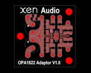
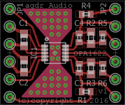
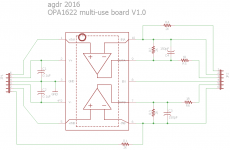
Here is my adapter board entry, in fabrication right now. I'm eager to test.
Mounting is via Mill Max 342 series pluggable board stacking pins on 0.1" centers, like 342-10-164-00-591000 or 592 for more height. The pins can be soldered on the other end or plugged into single row female collet header strips, or an IC socket. The rows are at a 15.24mm pitch so that a 24 pin socket could be cut in half.
By populating, shorting (0 ohm resistor), or leaving off various resistors it can be configured for any amp:
- non-inverting
- inverting
- balanced
- unity gain buffer
- parallel stack (includes pads for optional output balance resistors)
- pin-by-pin breakout
Attachments
Last edited:
- Home
- Vendor's Bazaar
- New Audio Op Amp - OPA1622