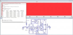
Sorry, it is not "my" simulation. Nevertheless, I am able to reproduce what you did and got your result.
You thought, that you replaced the transistor models by the command .include model.txt
As a matter of fact however, that didn't happen in the program. Because the default models are in LTSpice with the same name, the models were not replaced but the default transistor models got used despite your .include command. You can check it by pointing on the respective transistors in the schematic and then right click. I.e. for the IFPR240 (and the other MOSFETs) it will in your case show the manufacturer as "International Rectifier". However, if the correct models are used, it shows as manufacturer "VishIH1906" as given in the model.txt file.
Therefore your simulation with my file ends up with an enourmous idle current (check it,350mA) so that your THD results looks good at first glance, but is an artefact of the too high idle current resulting from a non adequate transistor model. I pointed to that issue in my earlier post.
I attached the result you would see, if the models were correctly replaced by those from my model.txt
Regards
Reinhard
Attachments
Last edited:
I had added the IRF model to the cmp file, but not to all of them.
Now I did, and the IRF comes as IH1906. But the THD is still 0.0195%
So it means I have to change all the models you are using to get a result you say it's the right one?
Thank you. I just need to see if the gain is inverting or not, for the simulation that uses ACE_BASS
I have changed the names of the transistor models to avoid mix-up with other models for these types. With the unique names there is no confusion anymore and the right model can be chosen safely.
I recommend to add below transistor models directly into the "standard.mos" file in the "cmp" folder in the "lib" directory of LTSpice. It will then show up and can be chosen with the new unique names listed when with pointing to the corresponding transistor in the schematic and selecting "pick new MOSFET".
I am using now unique names (attachments):
IRFP240VISH for Ian Hegglun's model for IRFP240 dd. June 2109
IRFP9240VISH for Ian Hegglun's model for IRFP2940 dd. June 2109
IRF610_IH for for Ian Hegglun's model for IRF610 dd. June 2109
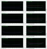
The result for the modified L7 with doubled NFB (half gain) and higher idle current (attached .asc) at 20kHz, 1W output into 4 Ohm load is THD=0.014% with LTSpice XVII (latest LTSpice version). Input amplitude is 204mVp for 1W output / 4 Ohm.
For the Original L7 (latest Version by LJM) it gives at 20 kHz, 1W output into 4 Ohm load, THD = 0.09%. Input amplitude is 106mVp for 1W output / 4 Ohm. Thus, the improvement with more NFB and higher idle current is very substantial (6x lower THD).
The old LTSpice version IV sometimes delivers a strongly deviating result with the same asc. file and same transistor models and sometimes works correctly. I couldn't figure out, why. The latest version XVII works consistently.
I also found that my first simulations used a different IRF610 model than the one I specified here. All of this contributed to deviations. The deviations however did not change the validity of principal conclusions and countermeasures and the crossover distortion of L7 at lower output unless modified.
Your THD 0.0195% result could be a consequence of running LTSpice with an older software version (not XVII) or it's still using a different model for IRF610 or both.
I recommend to add below transistor models directly into the "standard.mos" file in the "cmp" folder in the "lib" directory of LTSpice. It will then show up and can be chosen with the new unique names listed when with pointing to the corresponding transistor in the schematic and selecting "pick new MOSFET".
I am using now unique names (attachments):
IRFP240VISH for Ian Hegglun's model for IRFP240 dd. June 2109
IRFP9240VISH for Ian Hegglun's model for IRFP2940 dd. June 2109
IRF610_IH for for Ian Hegglun's model for IRF610 dd. June 2109
The result for the modified L7 with doubled NFB (half gain) and higher idle current (attached .asc) at 20kHz, 1W output into 4 Ohm load is THD=0.014% with LTSpice XVII (latest LTSpice version). Input amplitude is 204mVp for 1W output / 4 Ohm.
For the Original L7 (latest Version by LJM) it gives at 20 kHz, 1W output into 4 Ohm load, THD = 0.09%. Input amplitude is 106mVp for 1W output / 4 Ohm. Thus, the improvement with more NFB and higher idle current is very substantial (6x lower THD).
The old LTSpice version IV sometimes delivers a strongly deviating result with the same asc. file and same transistor models and sometimes works correctly. I couldn't figure out, why. The latest version XVII works consistently.
I also found that my first simulations used a different IRF610 model than the one I specified here. All of this contributed to deviations. The deviations however did not change the validity of principal conclusions and countermeasures and the crossover distortion of L7 at lower output unless modified.
Your THD 0.0195% result could be a consequence of running LTSpice with an older software version (not XVII) or it's still using a different model for IRF610 or both.
Attachments
Last edited:
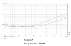
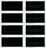
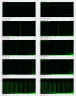
We see a considerable variation in simulated THD depending on the actual simulation models for the MOSFET parts. That's a weak spot and shows that in the MOSFET case simulated THD is less reliable.
Nevertheless trends are more valid if the circuit is changed in other parts as long as the MOSFET simulation models remain unchanged. So take simulated THD here with a grain of salt.
Keeping that in mind, I am attaching actual measured THD on my modified L7 circuits. As described, modification consisted of reducing the negative feedback resistor to half of its original value, which helps the input differential amplifier stage to counter distortion better. The other measure was changing the 9.1k/10k bias divider resistor pair to 10.00k/10.00k. In my experience, that was the most I could go without causing too much idle current/warming.
There are two THD curves in the attached plot. The upper one (higher THD) is typical for the modified L7 and represents measurements on three of my four modified L7 modules. The lower one (smaller THD) is a "lucky case" I found four one of my four modules. There is no known difference in the parts. I suspect that the "lucky case" represents by chance a well matched power MOSFET pair. I have no other explanation.
I don't have the THD of the non-modified L7 documented. I measured them also and I can assure that THD was (under same measurement conditions) for 1W output higher by a factor of 2-6 times as mentioned at the beginning of this thread. For 10W output power and more, the THD difference between original L7 circuit and modified L7 schematic decreased.
Best Regards,
Reinhard
Attachments
Last edited:
is it possible to have the schematic of the changes you made?We see a considerable variation in simulated THD depending on the actual simulation models for the MOSFET parts. That's a weak spot and shows that in the MOSFET case simulated THD is less reliable.
Nevertheless trends are more valid if the circuit is changed in other parts as long as the MOSFET simulation models remain unchanged. So take simulated THD here with a grain of salt.
Keeping that in mind, I am attaching actual measured THD on my modified L7 circuits. As described, modification consisted of reducing the negative feedback resistor to half of its original value, which helps the input differential amplifier stage to counter distortion better. The other measure was changing the 9.1k/10k bias divider resistor pair to 10.00k/10.00k. In my experience, that was the most I could go without causing too much idle current/warming.
There are two THD curves in the attached plot. The upper one (higher THD) is typical for the modified L7 and represents measurements on three of my four modified L7 modules. The lower one (smaller THD) is a "lucky case" I found four one of my four modules. There is no known difference in the parts. I suspect that the "lucky case" represents by chance a well matched power MOSFET pair. I have no other explanation.
I don't have the THD of the non-modified L7 documented. I measured them also and I can assure that THD was (under same measurement conditions) for 1W output higher by a factor of 2-6 times as mentioned at the beginning of this thread. For 10W output power and more, the THD difference between original L7 circuit and modified L7 schematic decreased.
Best Regards,
Reinhard
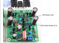
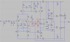
The only changes made are encircled in the attached schematic.
Please be aware that the transistors named 2N5551 are in reality NCC5551, which are electrically identical but have a different pin-out.They and the 1815 transistors are not changed, of course.
Only changes are:
1) A 2nd 33k resistor is soldered backside parallel to the already existing 33k resistor (negative feedback line).
2) The 9.1k resistor is replaced by a 10.00 k resistor. Care must be taken to match the resistance precisely (within +/- 0.5%) to the already existing 10k bias divider resistor (the one which has a common joint with the 9.1k). I.e. if the 10k bias divider resistor has an actual value of 10.13 kOhm, the one to replace the 9.1k resistor shall read between 10.08k min. and 10.18k max.
With the latest L7 boards by LJM, there is only one 33k reistor (only the one in the negative feedback) and only one 9.1k resistor (only in the bias divider) on the board, so that mixing up parts is not a concern.
NOTES:
1. Feedback Resistor
There are older versions of the L7, which have as negative feedback resistor instead of 33k (in this case there is 1k in series with the feedback foot capacitor of 470µF) 10k (in the latter case there is a 333R in series with the feedback foot capacitor of 470µF or 1000µF).
Note, that in both cases, the divider ratio 33k/1k, resp. 10k/333R is almost the same, namely 30-33. This results in a total amplifier gain of 29-30 (30dB).
The modification changes the ratio to 16.5k/1k, resp. 5k/333R, thus 16.5-15. Therefore the total gain of the modified L7 is reduced to 14-15 (24dB).
If the board is of the earlier generation with the 10k feedback resistor, then the parallel resistor shall be also 10k, of course.
2. Bias Divider Resistor
I noticed that there are early versions of L7 which have as bias divider pair 10k/11k instead of 9.1k/10k in the later version. If these are modified, it is also important, that both resistors of the bias divider are closely matched within +/- 0.5%. Either both 11k or 10k.
If you want to apply these changes, it's on your own risk, of course. No warranty from me. Just to mention, although it shall be clear anyway.
Idle current is increased, effective heat sink is important.
Attachments
Last edited:
The only changes made are encircled in the attached schematic.
Please be aware that the transistors named 2N5551 are in reality NCC5551, which are electrically identical but have a different pin-out.They and the 1815 transistors are not changed, of course.
Only changes are:
1) A 2nd 33k resistor is soldered backside parallel to the already existing 33k resistor (negative feedback line).
2) The 9.1k resistor is replaced by a 10.00 k resistor. Care must be taken to match the resistance precisely (within +/- 0.5%) to the already existing 10k bias divider resistor (the one which has a common joint with the 9.1k). I.e. if the 10k bias divider resistor has an actual value of 10.13 kOhm, the one to replace the 9.1k resistor shall read between 10.08k min. and 10.18k max.
With the latest L7 boards by LJM, there is only one 33k reistor (only the one in the negative feedback) and only one 9.1k resistor (only in the bias divider) on the board, so that mixing up parts is not a concern.
NOTES:
1. Feedback Resistor
There are older versions of the L7, which have as negative feedback resistor instead of 33k (in this case there is 1k in series with the feedback foot capacitor of 470µF) 10k (in the latter case there is a 333R in series with the feedback foot capacitor of 470µF or 1000µF).
Note, that in both cases, the divider ratio 33k/1k, resp. 10k/333R is almost the same, namely 30-33. This results in a total amplifier gain of 29-30 (30dB).
The modification changes the ratio to 16.5k/1k, resp. 5k/333R, thus 16.5-15. Therefore the total gain of the modified L7 is reduced to 14-15 (24dB).
If the board is of the earlier generation with the 10k feedback resistor, then the parallel resistor shall be also 10k, of course.
2. Bias Divider Resistor
I noticed that there are early versions of L7 which have as bias divider pair 10k/11k instead of 9.1k/10k in the later version. If these are modified, it is also important, that both resistors of the bias divider are closely matched within +/- 0.5%. Either both 11k or 10k.
If you want to apply these changes, it's on your own risk, of course. No warranty from me. Just to mention, although it shall be clear anyway.
Idle current is increased, effective heat sink is important.
GOOD
9k1 can be increased to 10K or 10k5
It can reduce the crossing distortion. This can be seen in the thd drop during the test.
But I don't think it makes much difference in practical application. As long as the radiator is big enough. Don't worry about using it.
10K is OK. 11K is OK. It's just a little hot.

Hi LJM,
I'm using LJM L15D PS boards for my dual mono setup. Here is my build post:
https://www.diyaudio.com/forums/class-d/87913-class-amp-photo-gallery-post6036470.html
I'm getting hissing noise from my bookshelf speakers (Monitor Audio BX2 - 90db) even when all input connections are disconnected from the amp. Could you please suggest what needs to be done here?
Thanks,
Saikat
L15D-PRO temperature
Hi,
I've just assembled two L15D-PRO boards bought off ebay.
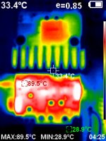
They are powered with +/-50v DC from a 1000W SMPS, and I have tested them okay (playing music just fine). However, I'm a bit confused by the heat produced by these modules. I was under the impression that these would be pretty much cold, but that is not the case with my modules. Attached are a IR Camera picture of my modules after idling for 10-15 minutes. The high temperature are the resistor just below D669 transistor.
Playing music (pretty loud though) increases the temperature of the heatsing by about 15 degrees, ending up at a total of just around 50 degrees.
Is this normal? I do not see any signs of oscillation on the output, however there are a constant sine wave of just above 500kHz (+/- 200mV), which I assume is the modulation frequency being present after the filter.
Best Regards
Hi,
I've just assembled two L15D-PRO boards bought off ebay.
They are powered with +/-50v DC from a 1000W SMPS, and I have tested them okay (playing music just fine). However, I'm a bit confused by the heat produced by these modules. I was under the impression that these would be pretty much cold, but that is not the case with my modules. Attached are a IR Camera picture of my modules after idling for 10-15 minutes. The high temperature are the resistor just below D669 transistor.
Playing music (pretty loud though) increases the temperature of the heatsing by about 15 degrees, ending up at a total of just around 50 degrees.
Is this normal? I do not see any signs of oscillation on the output, however there are a constant sine wave of just above 500kHz (+/- 200mV), which I assume is the modulation frequency being present after the filter.
Best Regards
Attachments
The 500KHz is just residual carrier is OK.
Could perhaps be fixed with a change of output filter components if it really worries you.
What is hot ? silicon can go upto about 150-200 degree's C before blowing.
50 degree's isnt the end of the world if thats the highest it gets even under high power output.
Could perhaps be fixed with a change of output filter components if it really worries you.
What is hot ? silicon can go upto about 150-200 degree's C before blowing.
50 degree's isnt the end of the world if thats the highest it gets even under high power output.
Hi,
yes, I know the silicon can handle way higher temperatures. I'm also running an Pass Aleph 5, which obviously run way hotter than this (Single Ended Class A).
The question is just if this is normal, or if I should digg deeper in finding the cause for this heat (if it is abnormal off course).
@carlmart: The 89.5 degrees are a 2w resistor of 1k. I do beleive that it is used to drop the voltage to the driver circuit. And, this is not an AB amp, it is a class D. I do beleive the L15D-PRO are the same as L15D, just with added speaker protection circuit on the board.
Been reading about the LJM 12-2 and L20 with interest.
I'm not savvy with soldering but can assemble stuff (LOL).
Was wondering if there are dealers out there (esp China) who provide kit modules, prepared cables etc etc for you to assemble your own L12-2 or L20 very much like what Hypex provides with their class D module DIY kit. Also caing made for such amps with suitable pre-drilled holes. Assembly intruction also.
Got any? This basically saves a lot on taxes because importing a finished amp incurs a 26% tax here whereas in kit for it is not taxed.
Thanks
Sorry: second try
Hello
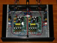
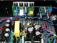
 This is my LJM-Audio L20.5 Amplifier.
I let pictures speak first.
https://www.diyaudio.com/forums/attachment.php?attachmentid=835638&stc=1&d=1587311061
https://www.diyaudio.com/forums/attachment.php?attachmentid=835639&stc=1&d=1587311061
https://www.diyaudio.com/forums/attachment.php?attachmentid=835640&stc=1&d=1587311061
https://www.diyaudio.com/forums/attachment.php?attachmentid=835641&stc=1&d=1587311061
https://www.diyaudio.com/forums/attachment.php?attachmentid=835642&stc=1&d=1587311061
@LJM Congratulations, with this Amplifier board you didn't promise too much

This is by far the best Amplifier I've ever built.
Thank you very much for that
Michael
Hello
This is my LJM-Audio L20.5 Amplifier.I let pictures speak first.
https://www.diyaudio.com/forums/attachment.php?attachmentid=835638&stc=1&d=1587311061
https://www.diyaudio.com/forums/attachment.php?attachmentid=835639&stc=1&d=1587311061
https://www.diyaudio.com/forums/attachment.php?attachmentid=835640&stc=1&d=1587311061
https://www.diyaudio.com/forums/attachment.php?attachmentid=835641&stc=1&d=1587311061
https://www.diyaudio.com/forums/attachment.php?attachmentid=835642&stc=1&d=1587311061
@LJM Congratulations, with this Amplifier board you didn't promise too much
This is by far the best Amplifier I've ever built.
Thank you very much for that
Michael
Attachments
Last edited:
- Home
- Vendor's Bazaar
- LJM Audio