US patent 5,612,646 (PDF version) discusses Berning's ZOTL circuitry (there are actually commercial amplifiers), where instead of using a regular output transformer, the output tube is fed through a high frequency ferrite transformer by the load and MOSFET bridge. Begning claims significant improvements in performance as the high frequency transformer supposedly has little impact on audio frequencies (the switching frequency is suggested around 250 kHz).
A diyaudio member, hifizen, suggested to me that a better design would, instead of having a switching bridge in the signal path, use AM modulation, thus still allowing the use of a high frequency transformer instead of a regular OTL.
I'd like to get some opinions and discussion on the pros and cons of these two suggestions, as well as implementation caveats to watch out for (I actually intend to build one or the other, and have procured appropriate ferrite cores).
Hi Nixie,
I think the AM modulation scheme will have a problem with demodulating the audio. If you use just diodes, then you have a single polarity only output. Could use a Mosfet bridge to get both polarities, but then you are back to the same parts count as the Berning scheme, and the zero crossings are at audio frequency instead of 250KHz.
A nice improvement on the Berning scheme can be had by going to a 2 phase arrangement with slowed down 250KHz edge transitions to avoid switching noise generation. (actually, no need to use such a high frequency with this appoach either) This requires doubling up the components, essentially two identical Berning units with the commutation diodes connected together at the tubes and the audio outputs connected together. Same LV power supplies. The switching of the two units is done 90 degrees out of phase using a set of Linear Tech ICs that control slew rates (both voltage slew and current slew controlled) to produce ultra low switching noise. The two overlapping phases allow one to stretch the transitions out with the diodes always selecting the phase at max voltage. No output filter (for HF suppression) required this way, and so no filter to interfere with feedback circuitry either.
One might also consider some other ripple free converter topologies such as the Cuk (pronounced shuk) converter. But more complicated.
Don
Hi Nixie,
The 2nd figure (actually labeled figure 1) is "doubled up" to handle the P-P case. For the two phase version, we double this again. Everything except the tubes, 70 & 90, and the power supplies, 28 & 88, get duplicated. Connect the two images together at the tubes and the power supplies, and the output, 44,46,42. The two osc in points , 61 & 62, would become the two 90 degree phase controls. Some simplifications are possible. For example, using center tapped primaries on the transformers, 50 & 51, allows cutting the number of transistors in half. (ie., CT config. versus full bridge config.) The output filter can now be just a "glitch" filter rather than a OSC freq filter, since there are no longer any "idle" crossover dead times at the OSC freq. in the output. (the 90 degree phases hand off control with overlap rather than dead time separation, so there are no longer any OSC freq. artifacts in the output)
Don
I did some experiments along these lines about 3 years ago. All that I can say is be prepared to offer up a lot of mosfets to the fire gods. I did manage to get sound, pretty good sound, but I got a lot more smoke. The thing would be playing along just fine, all fets were running cool, then bang, it would just blow up. I got tired of the smoke and gave up.
All of the cores that I used were robbed from computer power supplies. The circuit that I used seperated the power supply from the OPT. I was just working on a constant frequency OPT. The concept is outlined below. The best driver circuit used Microchip fet drivers in a floating arangement. I had a paper schematic, but I can't find it.
http://www.tubelab.com/SSopt.htm
Hi Tubelab,
Interesting work. Did you have snubber circuits on the drive FETs to protect them from leakage inductance voltage spikes?
I like the Berning design better since it avoids the need for the HV transistors, and even eliminates the HV supply too. I could never understand how he got a patent on it though, since the "DC transformer" idea has been around for some time.
Another, maybe even better, way to do it is to use two Cuk converters (one for each output polarity like the Berning design) with the two tubes in the HV sides and the output in series with the LV power supplies and converters, just like the Berning design.
The advantage here is the Cuk converter can do ripple free conversion without the need for a 90 degree phase add-on circuit, or a low pass filter, to cover the dead-time slots. (one can still do the slew rate limited switching to avoid HF noise at the cost of a little efficiency) In addition, it allows variable impedance transformation by PWM control besides the basic turns ratio transformation. (it still is ripple free at less than 50% duty cycle) Imagine being able to "tune" your OT impedance! Only requires 2 LV transistors too for a P-P design. But does require considerable mastery of the HF transformer design, which is more complicated than usual.
I plan to build one of these this Spring. I would like to get a PC board made eventually, with the Linear Tech controller IC for slew rate limiting of the switching, ie. RF quiet operation.
Don
Hmm, maybe you should start up a group order on the PCBs if the project looks promising.
With such variable impedance tuning, would it be possible to do it dynamically, so as to match perfectly the impedance curve of the load? That may be even better than the voltage-to-power amplifier mentioned here.
With such variable impedance tuning, would it be possible to do it dynamically, so as to match perfectly the impedance curve of the load? That may be even better than the voltage-to-power amplifier mentioned here.
Hi Nixie,
Hmmm, interesting idea on the dynamic impedance matching. I hadn't thought of that, but should be easy enough to do. The duty cycle, or PWM index, is just controlled by a voltage input to the PWM controller IC.
Trouble is that the audio signal is composed of multiple frequencies typically, and the speaker impedance varies with frequency. So there won't be an optimum impedance ratio to fit all the frequencies at once. Maybe for a multi speaker, frequency partitioned, system it would make sense to have it autotune.
If one used a constant power feedback system, as in the reference linked, it would likely skew the loudness of different frequencies playing simultaneously since it can only level the total power. One would need a powerful DSP chip to do frequency sensitive leveling in real time, where different frequency components would get scaled separately.
A "simpler" approach might be to just synthesize a fixed frequency selective filter with complementary characteristics to the attached speaker, and put it in the input signal path. That would work with an ordinary amplifier. Most practically done using a DSP chip again.
Don
I'm just dropping a note to this thread to say I think the patent has expired on Berning's ZOTL circuit.
https://www.google.nl/patents/US5612646
Not a lawyer but I think patents only go 20 years. I'm hoping someone makes a kit because I don't have the knowledge to put one together myself, or the money to buy one of his.
https://www.google.nl/patents/US5612646
Not a lawyer but I think patents only go 20 years. I'm hoping someone makes a kit because I don't have the knowledge to put one together myself, or the money to buy one of his.
Does look like it has expired. Filed Aug 1995, issued March 1997. 20 years cleared.
One of the unspoken issues with this scheme is that the XFMR leakage L is suffered at the HF carrier frequency. One needs to perfect low leakage winding technique on ferrites for this. Likely the best way would be a single layer per winding on toroids, with low turns ratio. Then use several toroids, with each HV secondary bridge rectified and the DC outputs summed for the tubes. The LV primaries get paralleled in two sets for the two switching phases. Two toroid sets needed then, one for each tube.
And then catch diodes across the Mosfets to dump leakage currents back into the LV supply(s). A low and high side driver IC might be used for driving the lower and upper (half bridge) Mosfets. (or a small gate driver ferrite xfmr, with two secondaries, the high side floats on the audio output) A HF low-pass filter on the output. Audio N Fdbk will have to handle the filtering phase shift.
There were several patent work-arounds posted way back (T multiplexed xfmrs or using a Circlotron configuration, even a resonant capacitive voltage multiplier; the T multplexed variant can do CFB, which the standard version cannot). Didn't seem to be much interest then. But maybe with a ready made PC board some activity could develop. There is a guitar amplifier using the technique. I think that is were it will catch on, cost sensitive applications.
Last edited:
Differential SMPS for ZOTL type amplifier
Hi there,
Sorry for reviving the thread, but I was wondering if I could use a PUSH-PULL converter from +/- 24Vdc to HV (like the car amplifier power supplies)? Using an offline 230 to HV and connecting the speaker in series with the primary is just asking for trouble.
My idea would be to use this +/- 24Vdc (or higher depending on the load impedance, switching frequency, etc) driven converter to power a one 24V primary at let's say 1Mhz (I would use 3F4 material from Ferroxcube) or 500Khz and use the 3F3 material... It's all a balance based on the necessary power, turns ratio, leakage inductance, coupling, etc dictated by the tube you will choose to use as the load (in my case it's the almighty 833A).
Because of the differential supply there will be only one primary which will be in series with the actual speaker, and then going to GND (midpoint of the +/- supply). To eliminate the switching ripple I could use a LC filter from GND to - of the speaker.
This way there will be a + to - swing of the converter current on the speaker load thus making it possible to have a class A2 drive on the power tube and in the primary have some Push-Pull driving the speaker from + to -
I want to avoid the two full bridges and two output tubes from the original patent.
I did not find the time yet to play with this idea in LTSpice but the weekend is pretty close. In the meantime... can you guys tell me if my concept seems flawed to you.
An 833A ZOTL amplifier is doable if you drive it in class A2 thus keeping the anode voltage to 850Vdc... ish
I have experience with SMPS design, classD design and I've recently designed and built an 4x6C33C OTL cyrclotron that will feed my Quad ESL 63 speakers (after I refurbish them completely)
So what do you think of this madness?")
Hi there,
Sorry for reviving the thread, but I was wondering if I could use a PUSH-PULL converter from +/- 24Vdc to HV (like the car amplifier power supplies)? Using an offline 230 to HV and connecting the speaker in series with the primary is just asking for trouble.
My idea would be to use this +/- 24Vdc (or higher depending on the load impedance, switching frequency, etc) driven converter to power a one 24V primary at let's say 1Mhz (I would use 3F4 material from Ferroxcube) or 500Khz and use the 3F3 material... It's all a balance based on the necessary power, turns ratio, leakage inductance, coupling, etc dictated by the tube you will choose to use as the load (in my case it's the almighty 833A).
Because of the differential supply there will be only one primary which will be in series with the actual speaker, and then going to GND (midpoint of the +/- supply). To eliminate the switching ripple I could use a LC filter from GND to - of the speaker.
This way there will be a + to - swing of the converter current on the speaker load thus making it possible to have a class A2 drive on the power tube and in the primary have some Push-Pull driving the speaker from + to -
I want to avoid the two full bridges and two output tubes from the original patent.
I did not find the time yet to play with this idea in LTSpice but the weekend is pretty close. In the meantime... can you guys tell me if my concept seems flawed to you.
An 833A ZOTL amplifier is doable if you drive it in class A2 thus keeping the anode voltage to 850Vdc... ish
I have experience with SMPS design, classD design and I've recently designed and built an 4x6C33C OTL cyrclotron that will feed my Quad ESL 63 speakers (after I refurbish them completely)
So what do you think of this madness?
I'm just dropping a note to this thread to say I think the patent has expired on Berning's ZOTL circuit.
US5612646A - Output transformerless amplifier impedance matching apparatus
- Google Patents
Not a lawyer but I think patents only go 20 years. I'm hoping someone makes a kit because I don't have the knowledge to put one together myself, or the money to buy one of his.
funny idea, not bad.
i wonder what is max freq of H2 /deuterium thyratrons.. because they coul fit into schematic nicely. Hg is max 200hz...
or maybe NOT tryratron, it seems to be made around "magnetic passive amplifier" .. tube is shorting the winding, lowering impedance and increasing load current
----
actually it could be possible just to use one tube for both halfwaves; but grid must be feeded by absolute signal value (incoming signal being rectified by bridge)
Last edited:
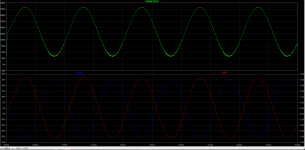
Update:
Some corrections from the last simulation where I have completely forgot about tube bias.
I hope it sheds some light on how this topology works. I will need to consult with some smarter people and try to get back with a closer to reality simulation.
Silviu
Some corrections from the last simulation where I have completely forgot about tube bias.
I hope it sheds some light on how this topology works. I will need to consult with some smarter people and try to get back with a closer to reality simulation.
Silviu
Attachments
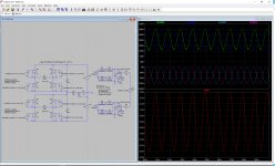
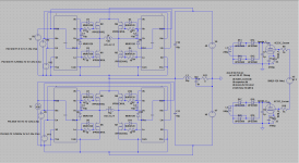
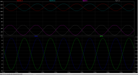
Update:
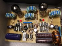
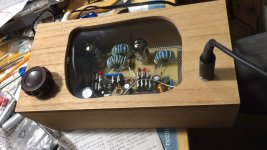
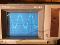
I managed to find some time and populated the schematic with real world parts and the results seem OK.
Unfortunately I don't really know if I'll start work on this project this year since I need to finish my 6C33C OTL Cyrclotron and my Balanced DHT Line stage and get my Quad ESL 63 panels refitted.
But I have all the parts for the DC/DC converters (I just need to wind the HF transformers).
In the meantime I have attached some screen shots.
Regards,
Silviu
Attachments
The 34kHz lowpass filter on the output seems a bit too close to the audio band for comfort, but that's easy to tweak. One major difference between the Berning circuit and the converter posted on the Tubelab site is the extra power supply on the secondary side in the former. If my understanding of the circuit operation is correct, the power to the speaker is actually being provided by this secondary-side supply, which really makes this a class D amplifier that's being amplitude modulated by a tube amplifier (instead of being modulated by the gate drive waveforms). On the other hand, the Tubelab circuit is what people in RF might call a "passive" upconverter and downconverter, and the power is actually being provided by the tube output stage. I don't know what kind of sonic differences this might lead to between the two designs, but I'm having a hard time convincing myself that the Berning circuit doesn't just approach typical class D performance as the THD from the tube stage gets lower and lower. Could you get the same sound signature from a tube preamplifier feeding a class D output stage?
- Home
- Amplifiers
- Tubes / Valves
- ZOTL and ferrites