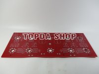
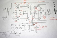
According to this the tubes for it are 2 x 6N9P, 2 x 6N8P, 4 x EL34/KT88 and 2 x 5Z3P. See: 1PC Push-pull amplifier PCB For EL34/KT88 | eBay
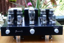
Maybe it's a (close) copy of one of the versions of the "Bewitch 6550".
Maybe it's a (close) copy of one of the versions of the "Bewitch 6550".
Attachments
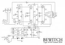
That schematic does not work at all. Look at the phase splitter for example. I has 100 ohms tail resistor ??
You've overlooked R2 and R3. The 100ohm is just fine tuning their contribution and providing the earth path.
kind regards
Marek
Maybe it's a (close) copy of one of the versions of the "Bewitch 6550".
PFL200,
Excellent detective work - I tried and failed to find anything useful! Is your day job being a detective?
")
Last edited:
Marek, could you clarify your comment. I don't get your point. That circuit simply can not work.
In this particular schematic the V1 should operate as a phase splitter.
Tell me from where does the upper halve V1b get the drive signal ?
Through the cathode, no?
Phase Splitters
V1a and v1b are in phase with each other as you point out, but they are not the phase splitter.
As I see it, the phase inversion happens at v2b because the v2b's share a common tail resistor and a signal fed along the bottom v2b . (The top two valves and the bottom two valves are direct coupled so conceptually they are each just one big valve with extra gain.)
The v1a valve provides gain, bottom v2b would be set up to add to it, top v2b (sic) inverts bottom v2b because they share a common tail resistor of r6 II r7 and v1b provides the bias point for top v2b.
Like all paraphase types, this will be hideously unbalanced with lashings of 2nd harmonic.
I expect it's set up like this because it is an adaptation of something totally different.
kind regards
Marek
You miss the direct coupling - V1 and V2 are not separate valves - V1 is just the first half of a Darlington where each V1+V2 is a single composite valve with a higher mu than either v1 or v2 on its own. Think of it as having a new combined plate curve, just like a Darlington transistor cannot be split. The phase inversion is at the grids of V2 and that feeds back to ground via v1a, rather than a signal at v1a driving the top (helpfully mislabelled) v2b.
The only reason I can see that a 100ohm resistor has been used in the tail of V1 is that 2k4 is not a readily available value for the desired cathode resistor, whereas it could be made easily from stock values this way.
kind regards
Marek
The only reason I can see that a 100ohm resistor has been used in the tail of V1 is that 2k4 is not a readily available value for the desired cathode resistor, whereas it could be made easily from stock values this way.
kind regards
Marek
...2k2 resistors on each cathode and then 100 Ohm common to ground, the second cathode will not get enough signal to make the two triodes act as a clean phase splitter.
Exactly. V1b does not have practically any signal voltage at its cathode, because the common tail resistor is far too small and in addition the 2k2 resistor together with that 100 ohms form a voltage divider that even reduce the signal voltage.
Typically the common tail resistor is some tens of kilo ohms. In high performance LTP phase splitters the tail resistor is replaced with high impedance CCS.
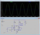
Attached the simulation of the circuit discussed. Green trace is the signal at the plate of V1a and blue at the plate of V1b. These two signals should have equal amplitude.
Clearly this circuit does not work as a proper phase inverter.
Attachments
Of course the V2 as it is a differential stage with relatively large tail resistor will balance the huge difference of its input signals, but still significant difference remains at the output of V2 stage. Therefore output tubes are driven with unequal drive signals and this unbalance finally must be corrected with GNFB. Hardly anybody prefer this kind of construction.
Much better results would have achieved with a single 6SL7 halve as voltage amplifier direct connected the 6SN7 LTP.
At the schematic discussed V1b has no function.
The output stage (6550) neither is optimal since output tubes have common cathode resistor.
Much better results would have achieved with a single 6SL7 halve as voltage amplifier direct connected the 6SN7 LTP.
At the schematic discussed V1b has no function.
The output stage (6550) neither is optimal since output tubes have common cathode resistor.
With the data found here and http://lampizator.eu/amplifiers/china/bewitch 6550/IMG_5581.jpg
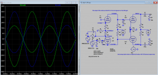
I'm able to sim more precisely, it' appeared all needed is unequal resistor in LTP will do well under full Gnfb, as some may found problem with NFB and have feedback disconnected becasue feedback makes unbalanced output worse as is.
I'm able to sim more precisely, it' appeared all needed is unequal resistor in LTP will do well under full Gnfb, as some may found problem with NFB and have feedback disconnected becasue feedback makes unbalanced output worse as is.
Attachments
- Home
- Amplifiers
- Tubes / Valves
- Schematic push-pull amplifier for EL34/KT88