Hi all,
I'm going to purchase some of Merlin's Universal PCBs to use, and, to try to extract some of his wisdom regarding the way he solved the design problem.
I know chassis layout is a huge part of building an amplifier so the way the PCB is laid out will also be critical. Avoiding ground loops, using star grounds sensibly is high on my priority list. I know ground planes don't really make sense at audio frequencies.
But other than that, are there any general advice for laying out PCBs for valve amplifiers? For example: track thicknesses, maintaining separation between signal carrying track and sources of noise, where to use metallisation, should certain tracks be separated along the front and back of the board?
I am mostly coming from guitar amplifier perspective so I will have a few gain stages, EQ, phase splitter, power section and power supply.
Quite a broad topic, I'm mainly interested in any wisdom I can gather before starting so I don't have to repeat mistakes others have encountered! But also knowing why to do things is a certain way is important I think.
Last edited by a moderator:
Ive been using PCB's for a few years now with tubes and have learned alot! Ive also been using ground planes as well. A few things I recommend would be large traces and pads particularly for the tube sockets, a minimum clearance of at least, 0.02" between traces, pads, and ground plane, minimum trace width of at least 0.05" for signal, and if one uses DC heaters, a trace width of 0.07" minimum, and one last thing if there any vias, make them larger than Your trace width, and I use hole sizes that are slighty larger than component lead width, its makes desoldering and removal much easier.
BTW, I only recommend ground planes only on boards with soldermask, if not, there is a clearence of 0.03" or larger.
BTW, I only recommend ground planes only on boards with soldermask, if not, there is a clearence of 0.03" or larger.
Last edited:
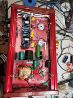
My only issue with PCBs is heat - both in terms of the PCB needs to be designed to allow airflow and the effect of heat on the joints. I have this mental picture of heat conducting down the pins of the tube socket causing joint fatigue as the PCB can't move in the same way as P2P. I've noted a number of PCB designs using short joining wires to the sockets, perhaps in the long term this is better..
Creep and clearance, also just as you would expect parallel tracks etc can couple etc.
Creep and clearance, also just as you would expect parallel tracks etc can couple etc.
A few tips:
1. Keep series grid resistors as close to the grid socket pin.
2. Keep anything of big signal "in phase" with the first grid far away. Any stray eletrical fields in phase are risks of positive feedback, hence oscillation.
3. If transformer or chokes are to be mounted on the PCB, give layout options for 90deg orientation.
4. Keep high AC or pulsating DC power supply stuff far away from small signal stuff, such as power transformer, rectifier + wiring and first choke, if any.
5. Do not mix PSU "dirty ground" with signal ground. Check some grounding literature.
6. Do not put electrolytic capacitors close to heating elements, such as tubes and anode resistors, as they will age earlier due to excessive heat.
7. Some tubes might benefit from, even need ventilation holes bellow them in the PCB.
8. Increase soldering surface area for elements that will be often mechanically stressed, such as connectors, potentiometers, switches, tube sockets, etc. Do the same for some heavy elements, such as big capacitors.
Thanks folks!
Denny, really interested to know more about when you use ground planes successfully. From what I understand there is a trade off between ground plane and star-ground. If significant current is flowing in the ground plane then there will be voltage drops and noise currents; star-ground minimises this but is more susceptible to magnetic induction. See answer here:
operational amplifier - Single point vs Ground plane, in audio OP AMP PCB layouts - Electrical Engineering Stack Exchange
Anyway, I don't want to get off topic! This is about gathering best practices, so thanks, I'm just trying to understand better.
It must be obvious to someone with more experience, but what do you mean that you only recommend ground planes with boards with solder masks?
Nick, Nigel, would be interested in some photos of those PCB with short leads. I don't like the idea of tube sockets on PCBs either, but I'm trying to be pragmatic. I must prefer to chassis moubt an hook up later. But decided keeping things simple is the best approach right now.
Old Hector, maybe we should just put a small robot arm inside the chaisse so it can rewire everything while I'm making a cup of tea") joking aside, yes would be cool. Sketch something up, I might take a look if I get the bug.
joking aside, yes would be cool. Sketch something up, I might take a look if I get the bug.
Denny, really interested to know more about when you use ground planes successfully. From what I understand there is a trade off between ground plane and star-ground. If significant current is flowing in the ground plane then there will be voltage drops and noise currents; star-ground minimises this but is more susceptible to magnetic induction. See answer here:
operational amplifier - Single point vs Ground plane, in audio OP AMP PCB layouts - Electrical Engineering Stack Exchange
Anyway, I don't want to get off topic! This is about gathering best practices, so thanks, I'm just trying to understand better.
It must be obvious to someone with more experience, but what do you mean that you only recommend ground planes with boards with solder masks?
Nick, Nigel, would be interested in some photos of those PCB with short leads. I don't like the idea of tube sockets on PCBs either, but I'm trying to be pragmatic. I must prefer to chassis moubt an hook up later. But decided keeping things simple is the best approach right now.
Old Hector, maybe we should just put a small robot arm inside the chaisse so it can rewire everything while I'm making a cup of tea
joking aside, yes would be cool. Sketch something up, I might take a look if I get the bug.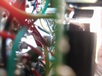
I was thinking of wavebourns' PCB for example - at the foot of the page:
https://www.diyaudio.com/forums/tub...riode-class-a2-driver-design.html#post6742046
https://www.diyaudio.com/forums/tub...riode-class-a2-driver-design.html#post6742046
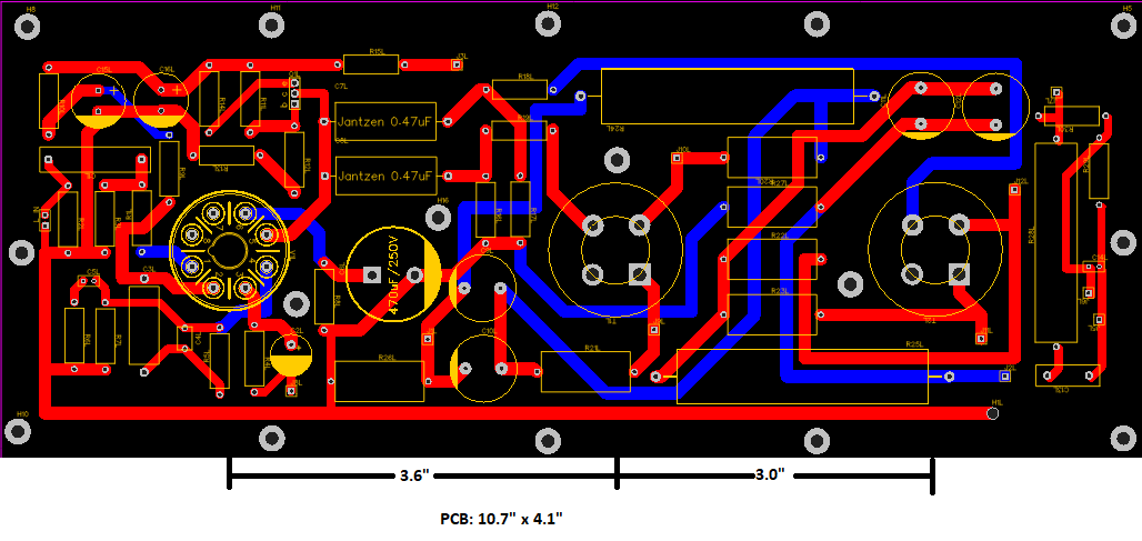
I wish there were more boards designed to fit over panel mounted sockets, i.e. with holes for the whole socket, so tubes with differing pinouts or heater voltages, or even bases (loctal instead of octal) can be substituted.
upvote from me on that. A big hole does interrupt the ground plane but there are ways to mitigate that by a 4 layer board to add back some copper. But the flexibility of a PCB that let's you rotate the panel mounted tube any which way or use different bases altogether is cool. I've seen commercial amps with these kind of PCBs, they hybrid out the tube sockets to wires not traces.
Remove a lot of the copper around the mounting / standoff screws, so that a brass standoff or wider screw head cannot possibly contact the plane or a trace and wind up connecting that to the chassis.
Remember the solder mask is not there to insulate anything, its only job is just to stop solder and provide a surface for printing.
Use thermal pads when the pad is on a copper plane be it a ground or power plane, a plane is hard to solder to without using excessive heat or time unless its a thermal pad. I learned this the hard way.
My general rule is, I never solder tube sockets directly to PCBs, even though it would be convenient and cost efficient.
I do not like heating/cooling cycles that cause mechanical stress. Also, such a way I can route components to minimize coupling between them and traces, and through the traces, instead of routing around the tube pin-out.
I do not like heating/cooling cycles that cause mechanical stress. Also, such a way I can route components to minimize coupling between them and traces, and through the traces, instead of routing around the tube pin-out.
Attachments
I like turret boards with chassis mount sockets mounted to them. They can make life easier in many ways. For grid resistors I put them directly from the socket to a turret post. All other connections I use jumpers from socket to turret. This gives you a clean framework to attach all the parts to eliminating movement and chance of shorts. Not cheap but worth it IMO.
My general rule is, I never solder tube sockets directly to PCBs, even though it would be convenient and cost efficient.
I do not like heating/cooling cycles that cause mechanical stress. Also, such a way I can route components to minimize coupling between them and traces, and through the traces, instead of routing around the tube pin-out.
Here is the video.
Wavebourn Edelweiss-3 Preamp Plus vacuum tube preamplifier drives 32 Ohm headphone loud - YouTube
It looks alright. I'd go Metric though... Putting a centre hole under the tube helps when laying out the chassis - you can use the board as a template.
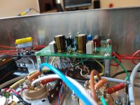
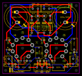
Here's a board I designed as a front end for a tube power amp. It runs 300V.
Your traces don't need to be so wide (except heaters etc) so you can get more clearance making them skinnier.
Here's a board I designed as a front end for a tube power amp. It runs 300V.
Your traces don't need to be so wide (except heaters etc) so you can get more clearance making them skinnier.
Attachments
- Home
- Amplifiers
- Tubes / Valves
- General rules for designing PCB for valve amplifiers