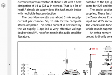
I was reading Menno van der Veen's article "Build 18 W Single Ended Valve Amplifier with Trans Technology" in the December 2019 issue of AudioXpress, went back and got his two part article from 2018.
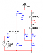
Menno uses the BSP135 as the driver for the valve output stage. I don't have BSP135 at the moment, some are on order from Mouser, but I do have LND150, a DMOSFet you can use between 1 and 3mA.
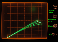
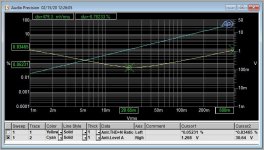
Here's the LND150 before it goes into pentode mode:
Menno uses the BSP135 as the driver for the valve output stage. I don't have BSP135 at the moment, some are on order from Mouser, but I do have LND150, a DMOSFet you can use between 1 and 3mA.
Here's the LND150 before it goes into pentode mode:
Attachments
Nice.
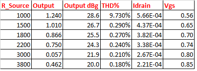
I think that the high reported THD at RS = 1,000 Ω is related to the R6 value of 100 kΩ. In a nutshell
⋅-⋅-⋅ Just saying, ⋅-⋅-⋅
⋅-=≡ GoatGuy ✓ ≡=-⋅
I think that the high reported THD at RS = 1,000 Ω is related to the R6 value of 100 kΩ. In a nutshell
R3 = 1000, op point = –0.600 V, at 0.600 mA
R3 = 1500, op point = –0.710 V, at 0.473 mA
R3 = 1800, op point = –0.760 V, at 0.422 mA
R3 = 2200, op point = –0.815 V, at 0.371 mA
R3 = 3000, op point = –0.900 V, at 0.300 mA
R3 = 3800, op point = –0.963 V, at 0.253 mA
So, it becomes perhaps-obvious that with a 60 volt B+ supply, R6's voltage drop with the given operating-point currents goes negative. LOL. The transfer curve of the depletion-mode MOSFET LND–150 isR3 = 1500, op point = –0.710 V, at 0.473 mA
R3 = 1800, op point = –0.760 V, at 0.422 mA
R3 = 2200, op point = –0.815 V, at 0.371 mA
R3 = 3000, op point = –0.900 V, at 0.300 mA
R3 = 3800, op point = –0.963 V, at 0.253 mA
i (mA) = (0.581 VG ⊕ 1.192)³
withR² = 0.99987
, from the curves given in the literature. That would be a pretty darn good fit.⋅-⋅-⋅ Just saying, ⋅-⋅-⋅
⋅-=≡ GoatGuy ✓ ≡=-⋅
BTW… while the curve-fitter is 'still hot', I did the BSP–135 depletion mode MOSFETs:
⋅-=≡ GoatGuy ✓ ≡=-⋅
i (mA) = ( 2.4665 VG ⊕ 4.4231 )³
so realistically, you're going to have to adjust some of the R3 and R6 values substantially, in order to have useful headroom.R3 = 1000, op point = -1.346 V, at 1.346 mA R6 = 21 kohm
R3 = 1200, op point = -1.370 V, at 1.141 mA R6 = 26 kohm
R3 = 1500, op point = -1.397 V, at 0.932 mA R6 = 31 kohm
R3 = 1800, op point = -1.419 V, at 0.788 mA R6 = 38 kohm
R3 = 2200, op point = -1.441 V, at 0.655 mA R6 = 46 kohm
R3 = 2700, op point = -1.463 V, at 0.542 mA R6 = 56 kohm
R3 = 3300, op point = -1.483 V, at 0.449 mA R6 = 68 kohm
R3 = 3900, op point = -1.499 V, at 0.384 mA R6 = 74 kohm
R3 = 4700, op point = -1.515 V, at 0.322 mA R6 = 90 kohm
R3 = 5600, op point = -1.530 V, at 0.273 mA R6 = 110 kohm
R3 = 6800, op point = -1.546 V, at 0.227 mA R6 = 130 kohm
R3 = 8200, op point = -1.560 V, at 0.190 mA R6 = 160 kohm
As it were...R3 = 1200, op point = -1.370 V, at 1.141 mA R6 = 26 kohm
R3 = 1500, op point = -1.397 V, at 0.932 mA R6 = 31 kohm
R3 = 1800, op point = -1.419 V, at 0.788 mA R6 = 38 kohm
R3 = 2200, op point = -1.441 V, at 0.655 mA R6 = 46 kohm
R3 = 2700, op point = -1.463 V, at 0.542 mA R6 = 56 kohm
R3 = 3300, op point = -1.483 V, at 0.449 mA R6 = 68 kohm
R3 = 3900, op point = -1.499 V, at 0.384 mA R6 = 74 kohm
R3 = 4700, op point = -1.515 V, at 0.322 mA R6 = 90 kohm
R3 = 5600, op point = -1.530 V, at 0.273 mA R6 = 110 kohm
R3 = 6800, op point = -1.546 V, at 0.227 mA R6 = 130 kohm
R3 = 8200, op point = -1.560 V, at 0.190 mA R6 = 160 kohm
⋅-=≡ GoatGuy ✓ ≡=-⋅
Last edited:
On that LND150 part ... 'proper' load resistors (setting a 1/2 B+ load V drop):
R3 = 1000, op point = -0.600 V, at 0.600 mA R6 = 51 kohm
R3 = 1200, op point = -0.649 V, at 0.541 mA R6 = 56 kohm
R3 = 1500, op point = -0.710 V, at 0.473 mA R6 = 61 kohm
R3 = 1800, op point = -0.760 V, at 0.422 mA R6 = 68 kohm
R3 = 2200, op point = -0.815 V, at 0.371 mA R6 = 82 kohm
R3 = 2700, op point = -0.871 V, at 0.323 mA R6 = 90 kohm
R3 = 3300, op point = -0.925 V, at 0.280 mA R6 = 110 kohm
R3 = 3900, op point = -0.969 V, at 0.249 mA R6 = 120 kohm
R3 = 4700, op point = -1.018 V, at 0.217 mA R6 = 130 kohm
R3 = 5600, op point = -1.063 V, at 0.190 mA R6 = 160 kohm
R3 = 6800, op point = -1.111 V, at 0.163 mA R6 = 170 kohm
R3 = 8200, op point = -1.156 V, at 0.141 mA R6 = 210 kohm
There's the update!R3 = 1200, op point = -0.649 V, at 0.541 mA R6 = 56 kohm
R3 = 1500, op point = -0.710 V, at 0.473 mA R6 = 61 kohm
R3 = 1800, op point = -0.760 V, at 0.422 mA R6 = 68 kohm
R3 = 2200, op point = -0.815 V, at 0.371 mA R6 = 82 kohm
R3 = 2700, op point = -0.871 V, at 0.323 mA R6 = 90 kohm
R3 = 3300, op point = -0.925 V, at 0.280 mA R6 = 110 kohm
R3 = 3900, op point = -0.969 V, at 0.249 mA R6 = 120 kohm
R3 = 4700, op point = -1.018 V, at 0.217 mA R6 = 130 kohm
R3 = 5600, op point = -1.063 V, at 0.190 mA R6 = 160 kohm
R3 = 6800, op point = -1.111 V, at 0.163 mA R6 = 170 kohm
R3 = 8200, op point = -1.156 V, at 0.141 mA R6 = 210 kohm
Maybe I am blind, maybe I am dumb, or both, but I fail to see what the "Menno Cell" has to offer, apart from a fancy name.
I just see a plain common-source voltage amplifier, followed by a plain source follower, without any smart mechanism for non-linearity compensation, impedance improvement or else.
It reminds me of very early crude linear IC's, like the TAA320 and others.
The rest of the 18W amplifier seems to be in the same style: the "very effective voltage doubler circuit" uses three times the number of diodes and 1.5x the capacitors compared to ordinary alternatives for exactly the same end result, except higher losses.
Maybe I missed something?
Maybe I am blind, maybe I am dumb, or both, but I fail to see what the "Menno Cell" has to offer, apart from a fancy name.
I just see a plain common-source voltage amplifier, followed by a plain source follower, without any smart mechanism for non-linearity compensation, impedance improvement or else.
It reminds me of very early crude linear IC's, like the TAA320 and others.
The rest of the 18W amplifier seems to be in the same style: the "very effective voltage doubler circuit" uses three times the number of diodes and 1.5× the capacitors compared to ordinary alternatives for exactly the same end result, except higher losses.
Maybe I missed something?
I must have missed something. Could you provide a link to the article that says “very effective voltage doubler circuit”? Thanks.
In this document:
https://www.mennovanderveen.nl/cms/...cember-AudioXpress_VDV-TRANS-SE18_artikel.pdf

https://www.mennovanderveen.nl/cms/...cember-AudioXpress_VDV-TRANS-SE18_artikel.pdf
Attachments
Maybe I am blind, maybe I am dumb, or both, but I fail to see what the "Menno Cell" has to offer, apart from a fancy name.
Not the first time he did that, I remember the 'E-choke', which is just a gyrator, not a new invention.
To be constructive, here are some ideas to spice up the circuit.
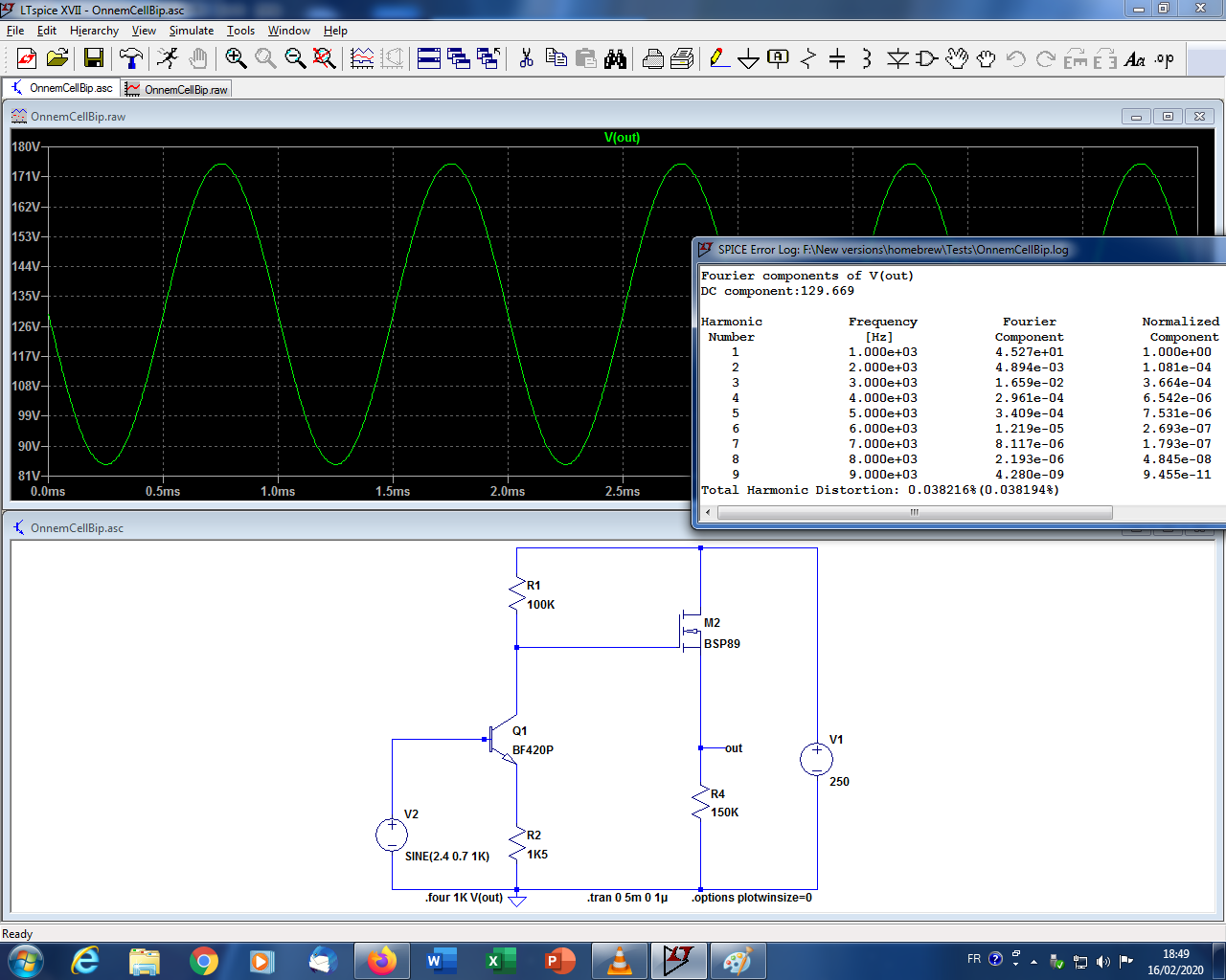
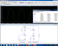
In this voltage amplifier example, the original circuit has a simulated THD of 0.47% with BSP89's as transistors and an output of ~90Vpp:
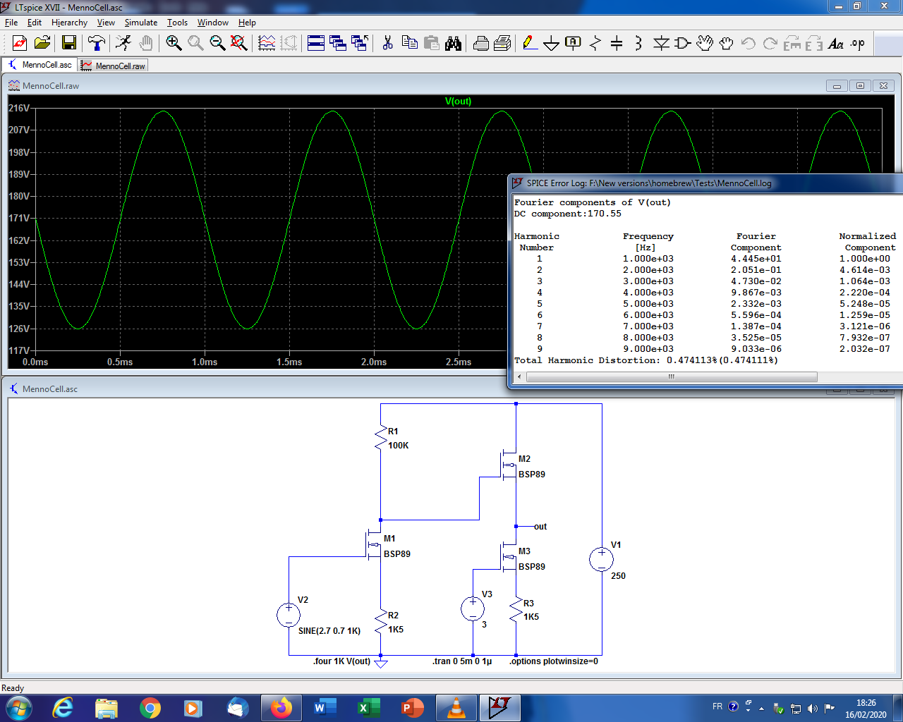
The distortion is mostly H2, caused by the non-linear modulation of Vgs, as in all simple amplifying stages of this kind.
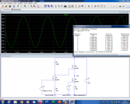
To improve the performance, there are a number of possible methods. One is to make the drain load non-linear in a homologous way.
In practice, the same transistor is wired as a resistance multiplier.
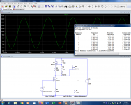
To make a zero-sum change, it is possible to lift the transistor from the output CCS: if the output current doesn't need to be especially high, it can be replaced by a resistor:
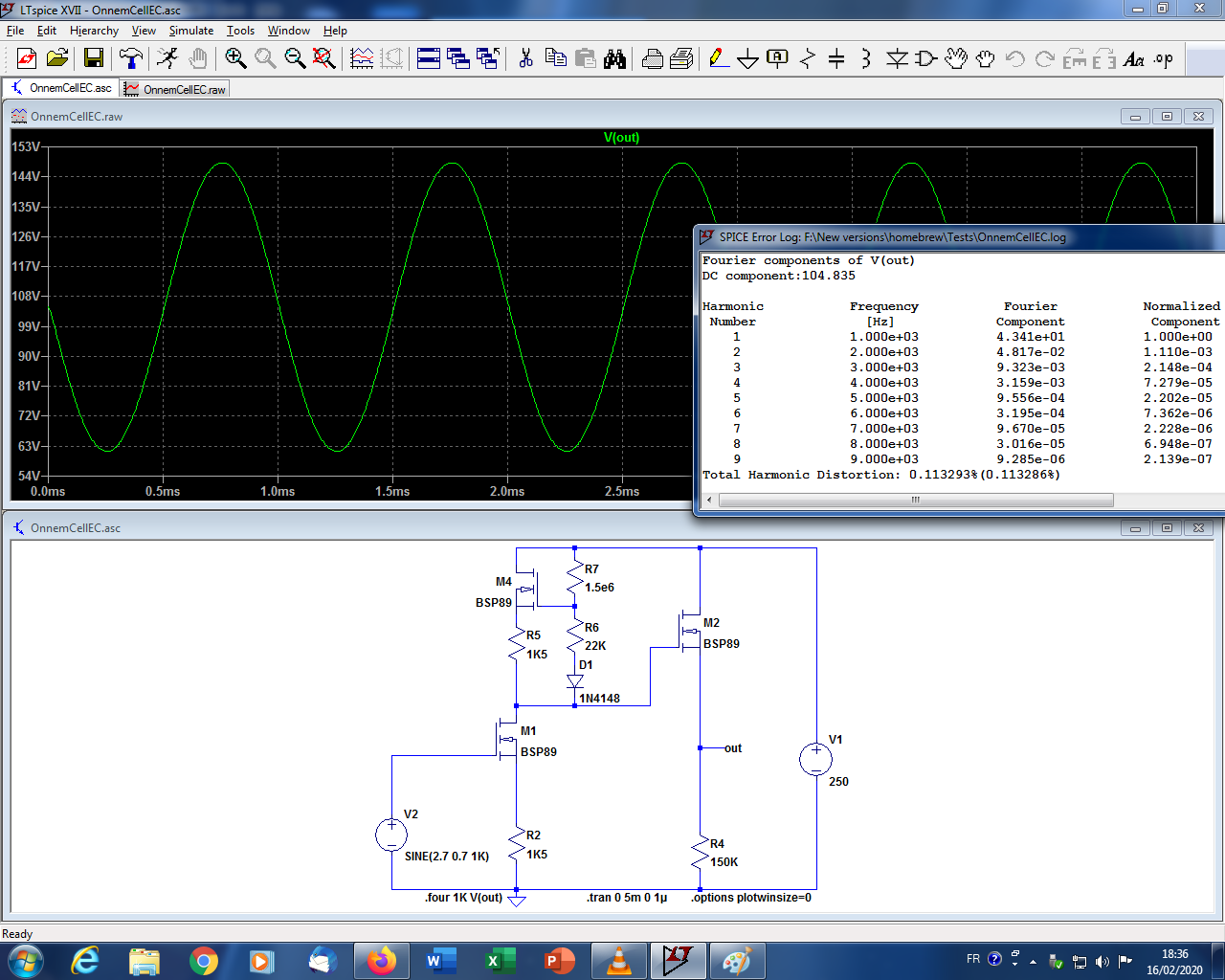
The mod simply rearranges existing components, and improves the THD but it kills the initial "cell" concept, unless the active load is seen as an additional cell.
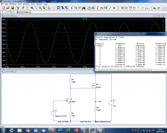
It is possible to keep the cell almost identical, and vastly improve its performance by replacing the MOS with a BJT, in this case a video-output transistor: the BJT has a smaller Vbe than the Vgs and has a higher transconductance, meaning a smaller proportion of non-linearity relative to the signal:
Of course, the BJT is a current-driven device, meaning a base current and a finite input impedance, but in this example, the input impedance is >150K, which is probably not going to be problematic
In this voltage amplifier example, the original circuit has a simulated THD of 0.47% with BSP89's as transistors and an output of ~90Vpp:
The distortion is mostly H2, caused by the non-linear modulation of Vgs, as in all simple amplifying stages of this kind.
To improve the performance, there are a number of possible methods. One is to make the drain load non-linear in a homologous way.
In practice, the same transistor is wired as a resistance multiplier.
To make a zero-sum change, it is possible to lift the transistor from the output CCS: if the output current doesn't need to be especially high, it can be replaced by a resistor:
The mod simply rearranges existing components, and improves the THD but it kills the initial "cell" concept, unless the active load is seen as an additional cell.
It is possible to keep the cell almost identical, and vastly improve its performance by replacing the MOS with a BJT, in this case a video-output transistor: the BJT has a smaller Vbe than the Vgs and has a higher transconductance, meaning a smaller proportion of non-linearity relative to the signal:
Of course, the BJT is a current-driven device, meaning a base current and a finite input impedance, but in this example, the input impedance is >150K, which is probably not going to be problematic
Attachments
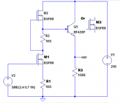
It isn't suitable as a direct substitute, because the ~infinite impedance of the SRPP makes the gain ~infinite and the DC bias unstable without external feedback, but the figure of merit of the circuit is very large: the THD is about the same as the original, but the gain is ~40 times larger.They are depletion fets, just like tubes.
So why not an SRPP followed by a "cathode" follower ?
Mona
In this sim, the depletion FETs have been emulated with a DC source in the gate:
This means that with properly applied FB, the THD could become 40x times smaller.
As the so-called "transamp" uses a semi-global FB scheme, it could in principle benefit from those properties.
However, it would be difficult to use in the 18W amplifier: it already uses 3 capacitors (C1, C2, C3) in the FB loop, and they have very awkward values, certainly because of the need to split the 3 poles sufficiently, and throwing an additional 52dB of gain into the game would certainly result in motorboating.
The DC stability issue would also be problematic.
In a completely revamped version, the circuit could do marvels though (with a large amount of FB, which might not be to everyone's taste, but that's another problem)
Attachments
- Status
- This old topic is closed. If you want to reopen this topic, contact a moderator using the "Report Post" button.
- Home
- Amplifiers
- Tubes / Valves
- The "Menno Cell" - Trans Technology