Help with B+ supply mod (gyrator?)
Dear community,
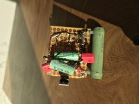
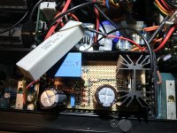
A few years ago, I got my AMC CVT3030 amp modified. One of the modifications was along the B+ supply to the tubes (gyrator?). While the acoustic result was very good, the execution of the mod, as you can see in the picture, was outrageously sloppy if not dangerous, to say the least.
Recently something got wrong with it while I was re-soldering a few shaky spots. Now I do not know how to fix this masterpiece which contains also some random components just hanging loose (!!!).
So I am thinking of reviewing and rebuilding it, possibly with your help.
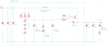
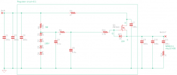
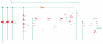
I am attaching a schematic I drew just by inspecting the piece of junk. As you can see in a couple of spots I do not even know if there is a connection or not. In the schematic I also included the large capacitors at the input (from the rectifier bridge) and output (rated 450V and 400V respectively).
Since this circuit is intended to provide a clean supply to the tubes I could also explore the alternative, possibly easier to implement, to eliminate the old mod and add the following Tentlabs module> Electronic Choke
What do you think? Would it be worth to try rework the old mod into a new one or just go with the Tentlabs module?
Thanks very much
Fabrizio
Dear community,
A few years ago, I got my AMC CVT3030 amp modified. One of the modifications was along the B+ supply to the tubes (gyrator?). While the acoustic result was very good, the execution of the mod, as you can see in the picture, was outrageously sloppy if not dangerous, to say the least.
Recently something got wrong with it while I was re-soldering a few shaky spots. Now I do not know how to fix this masterpiece which contains also some random components just hanging loose (!!!).
So I am thinking of reviewing and rebuilding it, possibly with your help.
I am attaching a schematic I drew just by inspecting the piece of junk. As you can see in a couple of spots I do not even know if there is a connection or not. In the schematic I also included the large capacitors at the input (from the rectifier bridge) and output (rated 450V and 400V respectively).
Since this circuit is intended to provide a clean supply to the tubes I could also explore the alternative, possibly easier to implement, to eliminate the old mod and add the following Tentlabs module> Electronic Choke
What do you think? Would it be worth to try rework the old mod into a new one or just go with the Tentlabs module?
Thanks very much
Fabrizio
Attachments
You don't have a Gyrator nor CSS. Looks to me you have a voltage regulator module. My guess is that it is used to regulate the screen voltage of the output tubes. Also I think the AMC CVT3030 uses only 4 output tubes. It uses silicon driver and preamp. The plate load Gyrator or CSS you have in mind won't work here. You best option is to fix what you have.
That's a regulator for sure.
I would be guessing that the suspect end of R8 would connect to C4 etc... at least I would want to RC filter my zeners (the noisy buggers... not to mention improved PSRR), and having 110k || 3.3k makes zero sense. C3 probably correct. R1 || R11 is a bit suspect, why would you need a precision gate stopper?
Also, I think L1 is just a wirewound resistor (47 ohm / 25 W).
Last edited:
Dear Allensoncanon and Sgrossclass,
Thanks a lot for your feedback! I will update the schematic and run it through spice to verify some details.
A couple more question:
- Can you help me understand how the output voltage is set?
- In terms of acoustic performance, would an E-Choke like the one from Tentlabs I mentioned in the first post, still be either a good alternate or addition to the voltage regulator?
Thanks again!
1. The Zener diodes set the rough output voltage (~400V). R8 to R10 fine tune it.Dear Allensoncanon and Sgrossclass,
- Can you help me understand how the output voltage is set?
- In terms of acoustic performance, would an E-Choke like the one from Tentlabs
2. Your amp looks to me only have 4 push pull output tubes which are already driving an inductive load (the output transformer). e-choke won't work there. Do you see another tube beside the 4 output tubes?
"at least I would want to RC filter my zeners" In which case perhaps C3 is across the zener string with R8 forming an RC filter with it, being connected where you have C3 connected at present.
Another thought occurs, is L1 really an inductor, it looks more like a big dropper resistor there to limit current.
If the circuit worked and improved the performance of the amp, why not just rebuild it on some tag board or make a proper "PCB" using single sided copper clad board. It's quick and easy to do with a dremmel and a fine bit.
It might help us advise you if we knew the circuit it replaced, voltage off the rectifier/smoothing cap and voltage/current requirement of the OP stage and drivers.
Andy.
I have to say… before looking at the circuit's picture, I looked at the schematic. And saw in parallel to the 120 kΩ resistors, a 3.3 kΩ resistor. Which, I thought "ought to pop". Sure enough… looking at the circuit portrait, said lil' resistor is popped, and gone. LOL. That was fun.
This is a series voltage regulator (not shunt-type). It is of the brilliantly-simple type … basically setting a very constant voltage for the MOSFET's gate, then letting the MOSFET proper do the source-follower function, much reducing power supply ripple, and further stabilizing the output to the series-of-gate-zenners voltage reference.
As another poster said, “if it is working, why not just do it better on a nice layout, etc?” (paraphrased)
But notes…
R8 is unnecessary.
R10 is unnecessary.
R9 value should be 100 kΩ, 2 watt
Between C4 and C5 should be a 1 kΩ resistor.
The 40 Ω R2 in front of C5 is of no utility.
The 15 kΩ in paralle to 2.2 kΩ in series to Q1 gate … is pointless.
Just use any resistor from 1.0 kΩ to 6.8 kΩ. Seriously.
D6 is a protective backstop. Keep it.
I'm not sure that L1 is what you think it is.
Could be a resistor.
But if it is an inductor, that's OK too.
Convention tho' would hold that the "output" of L1 (right side) would also be connected to ground via a medium-value capacitor (100 µF is good enough). This is not for filtering per se, but for reactance (impedance) reduction. The MOSFET can instantaneously deliver more juice with a small reservoir directly between its drain, and ground.
That's about all.
Just saying,
GoatGuy
This is a series voltage regulator (not shunt-type). It is of the brilliantly-simple type … basically setting a very constant voltage for the MOSFET's gate, then letting the MOSFET proper do the source-follower function, much reducing power supply ripple, and further stabilizing the output to the series-of-gate-zenners voltage reference.
As another poster said, “if it is working, why not just do it better on a nice layout, etc?” (paraphrased)
But notes…
R8 is unnecessary.
R10 is unnecessary.
R9 value should be 100 kΩ, 2 watt
Between C4 and C5 should be a 1 kΩ resistor.
The 40 Ω R2 in front of C5 is of no utility.
The 15 kΩ in paralle to 2.2 kΩ in series to Q1 gate … is pointless.
Just use any resistor from 1.0 kΩ to 6.8 kΩ. Seriously.
D6 is a protective backstop. Keep it.
I'm not sure that L1 is what you think it is.
Could be a resistor.
But if it is an inductor, that's OK too.
That's about all.
Just saying,
GoatGuy
To all, thanks for the additional valuable inputs. I truly appreciate your help!
@Allensoncanon> there's four tubes in total, two per channel. I am adding the complete schematics of the amp.
@Andy and Sgrossklass: I don't think there was an RC filter for the zeners. I (stupidly) soldered R8 to the input thinking it had come off. Instead it was just left hanging... As for C3 it's either connected to the input of left hanging. L1 should be indeed a 47ohm resitor. I wonder if I actually need that power rating.
Andy, as you can see on the schematics, the circuit is not replacing anything in particular. It just sits between the rectifier (480V open load) and the tube B+ supply which is originally set at 375V. As part of the mod at the time we changed the EL34 tubes to EL34G so I'm not anymore sure that's still the optimal B+ value.
After a closer look I just discovered R1 is not actually soldered to the gate...how can someone do such a sloppy work?
@GoatGuy: thanks so much for the very detailed analisys. I'm looking forward to making the changes you suggest. One more question> what do you think of the Tentlab module?
Attachments
Gents,
I rebuilt the regulator and I would like to test it before I put it back into the amp.
Unfortunately I do not have a 480V DC source. So I was planning to get the rectified transformer output (original B+ supply), put a resistive load on the regulator and check everything is in order before I connect the regulator output to the B+ on the tube modules.
Given the test setting above, I would turn on the amp and leave the B+ supply to the tubes floating.
Question> is this OK or would the tubes modules be damaged?
Thanks
Fabrizio
Regulator tuning
Dear all,
The regulator has worked very fine for a while and now I see some strange things happening. It might be related to the tuning of the tubes bias which I did after putting it in, but I am not completely sure.
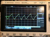
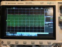
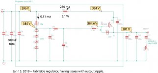
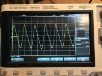
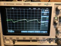
I am attaching the schematic and a few pics (AC) from the oscilloscope. As for the DC values here is the list:
Vin=396V
VR9-R4-D1-C4= 385V
Vd=384V
Vg=384.6V
Vout=381V
There might be something related to the RC bridges. In fact I had previously observed a similar behaviour where something like the charge and discharge of a capacitor affects the Mosfet gate and therefore the Vout. In that case I had succesfully bypassed R4.
At this point I miss some practical understanding on how to remediate. I hope we can solve this together - thanks a lot in advance.
Fabrizio
Dear all,
The regulator has worked very fine for a while and now I see some strange things happening. It might be related to the tuning of the tubes bias which I did after putting it in, but I am not completely sure.
I am attaching the schematic and a few pics (AC) from the oscilloscope. As for the DC values here is the list:
Vin=396V
VR9-R4-D1-C4= 385V
Vd=384V
Vg=384.6V
Vout=381V
There might be something related to the RC bridges. In fact I had previously observed a similar behaviour where something like the charge and discharge of a capacitor affects the Mosfet gate and therefore the Vout. In that case I had succesfully bypassed R4.
At this point I miss some practical understanding on how to remediate. I hope we can solve this together - thanks a lot in advance.
Fabrizio
Attachments
Dear all,
The regulator has worked very fine for a while and now I see some strange things happening. It might be related to the tuning of the tubes bias which I did after putting it in, but I am not completely sure.
Fabrizio
Yah… From the (rough) equation:
VP-P ≈ I / (C 2F) (amps / farads × 2 × Hertz)
VP-P ≈ 0.250 / (0.00088 F × 2 × 60 Hz)
VP-P ≈ 2.4 V
VP-P ≈ 0.250 / (0.00088 F × 2 × 60 Hz)
VP-P ≈ 2.4 V
I see that the ripple on VIN ought to be around 2.4 volts. (The 250 mA = 0.250 A came from 12 volt drop across the 47 Ω resistor.).
Thing is, that you're somewhat ironically working "too close to the margins" for the MOSFET, I think.
FIRST, ask yourself, “is 250 mA flowing out of this regulator, what I expect to be flowing out?” If "yes", then it is one heck of a power amplifier, taking about 100 input watts at near 400 volts. Bravo!
In any case though, to get the regulator MOSFET to actually regulate, you need MORE voltage on VD. The 47 Ω resistor is getting in the way. Its good protection, I suppose, but it is dropping too much. (And yes, this very well could be the result of you changing the BIAS of the output finals.)
So, as a simple experiment, simply bypass the 47 Ω resistor. You don't need to solder a wire-short-bypass, just use a well-insulated wire with alligator clips (insulated) on the ends. Bypassing the resistor will deliver ALL of the 396 VIN volts to the MOSFET, giving it some "margin" to work with.
I predict that as soon as you do that, unless some component is broken, that the output will stabilize to nice, flat DC, at around 381 volts.
The moral of that story would be … to use a smaller (like 15 Ω) safety resistor instead of 47 Ω.
Anyway, I've attached an annotated diagram.
GoatGuy
Attachments
Last edited:
Alternately… (if you want to keep the 47 Ω resistor), then choose different Zeners for the Zener chain. To be around 360 V total. Or, if you remember that the gate of the MOSFET consumes no power (at all), then you can go for a simple resistive voltage divider with the existing Zeners, to get a lower reference voltage.
You know, adding a 2 resistor divider between top of C₅ and ground, the "upper" resistor being 270 kΩ, the bottom one being 5.6 MΩ. This would give about 368 V to the gate of MOSFET, and represent only a 0.066 mA load to VIN
Just saying,
GoatGuy
You know, adding a 2 resistor divider between top of C₅ and ground, the "upper" resistor being 270 kΩ, the bottom one being 5.6 MΩ. This would give about 368 V to the gate of MOSFET, and represent only a 0.066 mA load to VIN
Just saying,
GoatGuy
Thanks a lot GoatGuy,
I should have realized that the total current drawn is just too high. Guess I am still rather rusty... I tested the regulator with a couple resistors (8k and 15k) as a load and everything works fine. So there should be no issue on the regulator alone.
Then, with the regulator connected, I measured how much current is drawn by the two tube modules (measured on R520) and by the preamp (measured on R332). According to the schematic attached, this should account for the total, which is around 28mA!
So now I am scratching my head on where the remaining current (~220mA) is going. Let me add a couple side problems I was going to check later on and which might be related or not:
- There s a low hum on the left channel only (independent of volume level) - The Direct/Phono/Normal knob makes a lot of noise everytime I switch it
Thanks
Fabrizio
PS: I forgot to add that bypassing the 47ohm resistor does not change how the regulator behaves
Attachments
I hope you find the source of "too much B+ current draw". It is important that you find the problem, since if it is being drawn by the output final tubes, well … a short life for them! ( 250 ma ÷ 4 ea ) × 380 V ⇒ 23,700 mW/tube. While you definitely have strong tubes, dissipating quiescent¹ 24 watts a bulb is quite a bit.
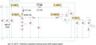
PS: In my annotated drawing, did I get the voltage values right? Here is another copy of it, with "ABCDEFG" annotations so that we can talk about test-points without having to refer to more cumbersome designations.
GoatGuy
________________________________________
¹ quiescent → the 'resting' current, power or voltage when no signal is passing thru circuit.
Attachments
Dear GoatGuy,
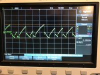
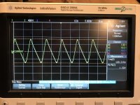
After several measuremens and talking with the AMC support I can confirm that the total current flowing through B+ is around 260mA and that the nominal B+ voltage is 375V.
So I modified the regulator to lower the output voltage to 375V by adding the voltage divider as you suggested. Unfortunately I observe the same behaviour described previously (see pics from oscilloscope) whether keeping R3 (47ohm) or bypassing it,
Referring to the new schematic attached here are the DC voltages
A= 400V
B= 387V
C= 389V (or C= 400V)
D= 376.4V
E= 376V
Now I have enough room for the regulator to work, however the problem persists.
Any idea on what to do next?
Thanks again,
Fabrizio
Attachments
OK… reading ( http:\\www.vishay.com\docs\91070\sihf840.pdf (repl \ with slash) ), it isn't too hard to figure out that the "turn on" for the IFR840 is about 3.5 to 4.0 volts (for ID of 250 ma). Something like that.
But your measurements of {D} and {E} are within a few tenths of a volt of each other. This implies that either the MOSFET is damaged, and its gate is broken, or, that the D5 diode has gone bad (near-short). Because "soldering is a pain", I would replace both at the same time, myself.
Leave the (not shown) voltage divider in place. It is a good idea.
The voltage you SHOULD be reading at {D} is as you say … around 275 V. The voltage at {E} though should be 4 volts or so below {D}. If the pair of MOSFET + D5 are working.
Also in the future — I cannot tell from your oscilloscope pictures at what points {ABCDE} they are being captured. Consider opening in a simple photo editor and "marking" with the test-point position from the schematic.
Yours, GoatGuy
(one last thought ... are you sure you have the D5 "pointing the right way"? Something also to check.)
Looks like a source follower buffered Zener supply to me.
Which is exactly what it is. However, there's a lot of extraneous stuff going on. With the filtering of the Zener stack before the MOSFET gate It should nominally be a dead silent supply, if nothing else.
That it is being tasked with supplying 250+ mA at 375 V quiescent is quite a thing. It must be for both channels, so 125 mA a channel. Yet that's still over 46 watts-a-channel in humming-along dissipation. And, granted, some of that 375 ought to be going to prior stages, the VAS and compliment inversion and so on, but still … lots'o'watts.
Just saying, GoatGuy
- Status
- This old topic is closed. If you want to reopen this topic, contact a moderator using the "Report Post" button.
- Home
- Amplifiers
- Tubes / Valves
- AMC CVT3030