Hi there,
As I am going to test some tube concepts, I felt the need to build a dedicated supply, capable of supplying all the essential voltages from a single box.
Of course, I already own a sufficient number of low and high voltage supplies, and in theory I do not need anything more, but having separate supplies is not really practical, except for a one-off.
I have included one main HV supply, capable of providing 150V DC to 400V DC at 500mA (0 to 450V with additional patching), many heater voltages and a grid bias, adjustable from 0 to -100V DC.
All the outputs are independent and completely floating.
Initially, I intended to use 3 or 4 traditional transformers from my stock, but I quickly realized that I would need more than that, because of the need to generate a vast number of heater voltages: my stock of tubes comprises E-series, P-series, U-series plus a number of US types.
I could have wound the 50Hz transformer myself, but that's something I hate, and ordering a complex, custom type would be expensive.
In the end, I settled for a crude switching supply: I also need to wind the transformer myself, but at least the numbers of turns are ridiculously low.
I kept the same philosophy as for a 50Hz transformer: there is no PWM control, and the heaters also operate directly from the AC.
I did this for a number of reasons, mainly heater-related: there are many windings, with many taps, and it would be unpractical to use as many rectifiers+filters.
In addition, I wanted to have the option of combining any winding to any other, including in subtractive mode, to create additional voltages, something impossible with DC supplies.
And finally, having heaters operating in DC and without an ohmic link between the two terminals didn't please me much.
The supply is not PWM-regulated, but it has a form of (crude) regulation.
It is necessary, because once the input voltage is (peak) rectified and filtered to feed the converter, it becomes significantly more load-dependent than the AC input.
Initially I had opted for a frequency-based control, but I encountered unexpected problems and had to turn to an even cruder phase-control of the mains input.
More on that later.
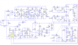
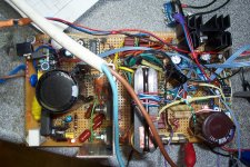
Here are the schematics and a few pics, but first, a warning: do not attempt to clone this project in the current condition: it has issues.
Why am I publishing it then?
For two reasons:
-One is egoistic: when I publish a project, I document it much more thoroughly then I would do it for just myself, and I can find it and retrieve it easily using the forum tools, in case I need to fix or modify it.
-The other is that most of the project is sound and useful, and it could easily be corrected if the right options were taken from the start.
In addition, some of the circuits and principles used work quite well, and could easily be useful in other, completely different projects, for example the overload protection scheme based on a non-linear ballast, or the grid supply circuit based on a Rush cascode: it is a simplistic, yet protected and LDO regulator, capable of supplying from 0V to the maximum voltage with decent performances.
As I am going to test some tube concepts, I felt the need to build a dedicated supply, capable of supplying all the essential voltages from a single box.
Of course, I already own a sufficient number of low and high voltage supplies, and in theory I do not need anything more, but having separate supplies is not really practical, except for a one-off.
I have included one main HV supply, capable of providing 150V DC to 400V DC at 500mA (0 to 450V with additional patching), many heater voltages and a grid bias, adjustable from 0 to -100V DC.
All the outputs are independent and completely floating.
Initially, I intended to use 3 or 4 traditional transformers from my stock, but I quickly realized that I would need more than that, because of the need to generate a vast number of heater voltages: my stock of tubes comprises E-series, P-series, U-series plus a number of US types.
I could have wound the 50Hz transformer myself, but that's something I hate, and ordering a complex, custom type would be expensive.
In the end, I settled for a crude switching supply: I also need to wind the transformer myself, but at least the numbers of turns are ridiculously low.
I kept the same philosophy as for a 50Hz transformer: there is no PWM control, and the heaters also operate directly from the AC.
I did this for a number of reasons, mainly heater-related: there are many windings, with many taps, and it would be unpractical to use as many rectifiers+filters.
In addition, I wanted to have the option of combining any winding to any other, including in subtractive mode, to create additional voltages, something impossible with DC supplies.
And finally, having heaters operating in DC and without an ohmic link between the two terminals didn't please me much.
The supply is not PWM-regulated, but it has a form of (crude) regulation.
It is necessary, because once the input voltage is (peak) rectified and filtered to feed the converter, it becomes significantly more load-dependent than the AC input.
Initially I had opted for a frequency-based control, but I encountered unexpected problems and had to turn to an even cruder phase-control of the mains input.
More on that later.
Here are the schematics and a few pics, but first, a warning: do not attempt to clone this project in the current condition: it has issues.
Why am I publishing it then?
For two reasons:
-One is egoistic: when I publish a project, I document it much more thoroughly then I would do it for just myself, and I can find it and retrieve it easily using the forum tools, in case I need to fix or modify it.
-The other is that most of the project is sound and useful, and it could easily be corrected if the right options were taken from the start.
In addition, some of the circuits and principles used work quite well, and could easily be useful in other, completely different projects, for example the overload protection scheme based on a non-linear ballast, or the grid supply circuit based on a Rush cascode: it is a simplistic, yet protected and LDO regulator, capable of supplying from 0V to the maximum voltage with decent performances.
Attachments
The main purpose of this project is to emulate the power-transformer side of things, not as a substitute for other internally generated voltages or bias, which is generally the case for G2 (not always, of course: you will always find exceptions): it is most of the times derived in some way from the main HT rail.
I included a negative grid bias, because when it is present, it requires such an additional winding+rectifier. The -100V is arbitrary anyway: since the supply is floating, it could also be used as a +100V supply, or referenced to any other voltage. The 100V value itself is purely arbitrary too: because the regulator can operate at a voltage determined only by the input voltage and the breakdown voltage of transistors, it could be made higher and serve as a G2 source, or any other role in fact.
I didn't care to go that far, because I still have my regular lab supplies as a complement, for the rare cases when I will need it.
How about pentode screen supplies?
In most audio, screen is derived "inside the amplifier". You have 400V for plates, a 2K resistor, cap, here's your 360V for screens.
There are other deals. 6146 will give gobs of current at Vg2 near 200V, and the plate will stand over 600V. Ig2 is very variable on dynamic signal or loading so a dropping-resistor won't do. RF transmitters (and medical devices) generally gave it a separate supply. Ampeg VT40 ran 595 V on plates of EL34, and originally ran G2 this hot, and the tubes didn't last; the later VT40 has a 285V Vg2 supply. Most 100 Watt 6550 and 8417 amps take 600V for plates and 300V for G2 (conveniently derived with Si diodes, often as a doubler).
It is *impossible* to build any single supply box for "any/all" tube amp projects. I've always felt that such a project just delays actual tube-cooking. But it is an interesting project in its own right.
The core of the circuit is a classical and dumb (no PWM) half-bridge converter, composed of M1 and M2 and driven by the CD4046.
A number of components on the driving side have become redundant, because of the switch from frequency-control to phase-control: the frequency was supposed to vary between 30 and 70kHz, controlled by the feedback optocoupler.
After the switch, I found it simpler to leave all the components in place, because they couldn't be just removed without impacting the switching frequency which is now fixed at 30kHz, but substituting any other 30kHz squarewave generator would be easy enough.
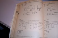
Initially, the frequency control had to work in combination with the deliberately high leakage inductance of the transformer: it is a U-core shape (see data below, 3C6 material), and the primary and secondary windings are on opposite legs, which results in a extremely high leakage. To give an idea, the primary magnetizing inductance is ~8mH, but the leakage inductance is ~720µH.
The way it worked is that the frequency was lowered as needed by the load. The ballasting effect of the inductance provided an overload/short protection... But it also raised unacceptably the internal impedance of the supply, which is why the series capacitors were made small enough to cancel the inductive reactance at 30kHz (C10 to C13).
This also improved the effectiveness of the frequency control, thanks to the resonance.
Of course, if the ballasting impedance is completely cancelled, the protection effect is equally lost, but here the clever part of the circuit comes into play: the series capacitance is split into two parts: C10/C11 and C12/C13.
The C10/C11 section is completely ordinary, but C12 and C13 are returned to the supply rails via recuperation diodes D10 and D11.
When the resonance current becomes high enough, the voltage at the junction of C12 and C13 tries to exceed the supply rails, and the diodes conduct for a part of the cycle, returning the reactive power to the supply and damping the resonant circuit, thus limiting the real power transfer.
The capacitors are calculated to limit the power at 300W: when the load tries to exceed that level, the current increases, but the voltage decreases accordingly, keeping the total output power at 300W, until the current reaches ~3 times its nominal value.At this point, the current remains ~constant, even for a dead short.
Three times the nominal current value is of course too high for permanent operation (it means ~10 times the dissipation in the MOSfets Rdson and the windings), but it is tolerable for seconds or even tens of seconds, the time to melt a fuse.
An ordinary converter would either need to be hugely overdimensioned to be able to melt a fuse safely, or have an explicit current protection, with a sensing resistor, etc. This scheme is inherent, implicit, and therefore less prone to failure. It also tolerates brief shorts or near-shorts, like the inrush current of a cold tungsten filament, or the charging of a filter cap.
Everything looks nice and dandy, yet there was a fly in the ointment...Where was it?
A number of components on the driving side have become redundant, because of the switch from frequency-control to phase-control: the frequency was supposed to vary between 30 and 70kHz, controlled by the feedback optocoupler.
After the switch, I found it simpler to leave all the components in place, because they couldn't be just removed without impacting the switching frequency which is now fixed at 30kHz, but substituting any other 30kHz squarewave generator would be easy enough.
Initially, the frequency control had to work in combination with the deliberately high leakage inductance of the transformer: it is a U-core shape (see data below, 3C6 material), and the primary and secondary windings are on opposite legs, which results in a extremely high leakage. To give an idea, the primary magnetizing inductance is ~8mH, but the leakage inductance is ~720µH.
The way it worked is that the frequency was lowered as needed by the load. The ballasting effect of the inductance provided an overload/short protection... But it also raised unacceptably the internal impedance of the supply, which is why the series capacitors were made small enough to cancel the inductive reactance at 30kHz (C10 to C13).
This also improved the effectiveness of the frequency control, thanks to the resonance.
Of course, if the ballasting impedance is completely cancelled, the protection effect is equally lost, but here the clever part of the circuit comes into play: the series capacitance is split into two parts: C10/C11 and C12/C13.
The C10/C11 section is completely ordinary, but C12 and C13 are returned to the supply rails via recuperation diodes D10 and D11.
When the resonance current becomes high enough, the voltage at the junction of C12 and C13 tries to exceed the supply rails, and the diodes conduct for a part of the cycle, returning the reactive power to the supply and damping the resonant circuit, thus limiting the real power transfer.
The capacitors are calculated to limit the power at 300W: when the load tries to exceed that level, the current increases, but the voltage decreases accordingly, keeping the total output power at 300W, until the current reaches ~3 times its nominal value.At this point, the current remains ~constant, even for a dead short.
Three times the nominal current value is of course too high for permanent operation (it means ~10 times the dissipation in the MOSfets Rdson and the windings), but it is tolerable for seconds or even tens of seconds, the time to melt a fuse.
An ordinary converter would either need to be hugely overdimensioned to be able to melt a fuse safely, or have an explicit current protection, with a sensing resistor, etc. This scheme is inherent, implicit, and therefore less prone to failure. It also tolerates brief shorts or near-shorts, like the inrush current of a cold tungsten filament, or the charging of a filter cap.
Everything looks nice and dandy, yet there was a fly in the ointment...Where was it?
Attachments
It is indeed, as are a number of components used in the switcher. It must have been introduced 40 or 50 years ago, for B/W TV applicationsYour transformer's core is of the same type as a flyback transformer's in old CRT TV's, isn't it?
I opted for this one because it made it easy to create the large leakage inductance required, and because the winding window is huge, and easily accommodates the large number of windings and taps.
Choosing the number of primary turns presented an unusual difficulty: it is normally based on the peak induction tolerated by the core, but here, the resulting V/turn constant would have been extremely large, and for the heater windings, the granularity would have been much too coarse.
On the other hand, I wasn't enthusiastic about winding hundreds of turns: I opted for a tradeoff: 2.25V/turn.
This makes most of the voltages slightly off, too high or too low, but for heaters, nothing intolerable.
In addition, if I need a particular voltage to be exact, I can always resort to the fine adjustment capability.
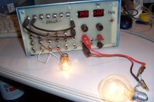
During the debugging/development phase, I made the tests mostly under medium, high, and over-load conditions.
When I was finally satisfied, the supply seemed to be stable, fault tolerant and well-behaved, and the simplistic regulation was able to reject most of the 100Hz ripple.
I then proceeded to more general tests. The output rectifier/filter block was connected to the 350V tap, but apart from the bleeder there was no load connected.
I immediately noticed that the bleeder's pilot LED was shining extremely brightly, which caught my attention. I then realized that the 120µF/450V cap was getting warm.
I immediately pulled the plug, of course, and measured the residual voltage on the cap: almost 600V!!!
Had I waited a few more seconds, the cap would certainly have blown up....
A bit shaken by the experience, I repatched the voltage to 150V, and this time I had the voltmeter already connected to the cap when I applied the power.
To my surprise, the voltage climbed quickly and crept towards 600V.
This puzzled me: I had imagined it had to do with ringing effects, but the voltage looked impossibly high.
In the end, I disconnected the output rectifier, but even so, the voltage was present and kept exceeding all reasonable limits.
This made me think that I had miswired something, but I wasn't able to find anything wrong.
I finally had an illumination, and disconnected the 0V output of the winding to the rectifier: the voltage was gone, at last....
The culprit was the electrostatic screen connection: to root out any possible CM emission, the HV secondary is fully sandwiched between two screens, and the screens are connected to the 0V DC output, but the screens to winding capacitance is relatively large, around 200pF, and combined with one arm of the rectifier bridge, it forms a voltage multiplier.
In an ideal world, with capacitances balanced and no ringing at all, the AC screen voltage should be 200V, and after doubling it would result in a maximum of 400V DC at the output, but as the screen capacitances are significantly imbalanced and some ringing is present, the voltage could rise to much more than that.
At this point, I felt stuck: I couldn't use the screens, but without them the supply would be practically useless.
If I had opted for center-tap windings+rectifier, there would have been no such problem, because of the galvanic connection between the windings and the ground, but I had rejected that configuration from the start, because it was less flexible: it would have complicated the patching and made series-connection of random windings impossible.
Now, the transformer was wound, and I didn't want to restart from scratch....
Attachments
Last edited:
After some serious thinking, I realized that it would be possible to save the project without too many tradeoffs or complications: even left floating, the screens already play an important part of their intended role: they suppress the local electrostatic fields generated by the windings.
The other part is to render the windings+screens unit neutral with respect to the ambient space and the output, in other words they have to suppress any common-mode signal generated between the transformer and the DC output.
This normally requires a hard connection between the screens and the output ground (or at least via a Y-like capacitor).
However, if the screens to windings capacitances are balanced, the screens will behave like a virtual center-tap, and if the rest of the circuitry (rectifier) is balanced too, no common mode will exist between the transformer and the DC output.
Here, one problem remains though: there are different taps to the winding, and exact cancellation will only happen for one setting.
This means that for other settings, either a residual CM will be present (if the screens are left floating) or parasitic charge will be pumped into the output (if the screens are tied to the 0V).
The final solution I adopted was to balance the screens by adding C1 (in the second schematic), and tie them to the output ground through a 47pF capacitor (C3).
This solution is not perfect of course, but it is an acceptable tradeoff: the charge injection is low enough to be managed by the bleeder, and the common-mode HF perturbations remain at an innocuous level.
Was I out of woods?
Not quite...
Now that the "ghost" voltages were mostly gone, another problem surfaced, and once again, the main culprits were .... the screens.
Under no-load conditions, the output voltage kept climbing until regulation was lost.
This time, the voltage posed no danger to the filter cap, but having no regulation is not acceptable.
I quickly saw that the overvoltage was caused by ringing.
In a normal, lone winding, the capacitance of an orderly winding, even a HV one is relatively low, and most of it is virtual and results from transmission line effects, but here, one screen was in full contact with the first layer and the other with the last layer.
Connecting the screens together was like having the first and last layer directly in contact, adding a huge physical capacitance to the regular one.
This meant that the ringing was much harder to tame, requiring a lot of energy dissipation in a snubber or similar circuit.
The problem was also made much worse by the regulation: because the voltage became too high, the regulation tried to increase the frequency, but this increased the amount of power delivered by the ringing: for low- or no-load, the regulation was reversed.
The servo would have had to take the load into account, and reverse its polarity at light loads... a control nightmare.
Wisely, I opted for a more realistic solution: I made the opto feedback work as a shunt regulator when the limits were exceeded: up to 1~2mA, the optocoupler worked normally, but when this didn't suffice, the current would increase to 50 or 100mA, to act as a bleeder on the 150V used for the servo feedback (and part of the output string) and bring the voltage under control.
The fix worked rather well, with the regulator transitioning seamlessly from opto to shunt regulation.
There was an obvious drawback though: this fix increased the no-load dissipation by 10 to 15W, something I found hard to swallow.
In the tube era, this would have been perfectly acceptable, but not in 2018.
In the end I had to scrap the frequency control, shunt reg, etc, and I fell back on a prehistoric but proven solution: phase control of the mains.
It is not elegant, it cannot remove the 100Hz ripple, but at least it works, and can be implanted without too much disruption.
Circuit description:
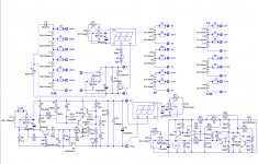
The controller for the main converter is a CD4046 PLL.
I had opted for this IC because it included a convenient VCO, but the final version doesn't make use of the frequency modulation, and any fixed 30kHz oscillator would do the same job, just more simply.
The auxiliary supply for this controller is derived from a capacitive supply, operating at a relatively large voltage (60V), to minimize the size of the dropper capacitor, 220nF here.
The 12V output is translated to 60V by two totem-pole transistors Q2 Q3, driving the gate-drive transformer.
The converter has a classical half-bridge topology, but with a twist: normally, the impedance of the coupling capacitors at the running frequency is negligible, but here their impedance is significant to compensate for the deliberately high leakage inductance.
The compensation of C10 to C13 is exact at 30kHz, but since the capacitors are split and recuperation diodes are added, the compensation ceases to operate when the primary current exceeds 3 x Inom.
This mechanism provides the first protection means in case of a short or overload.
It is not meant to work alone: after some time, ms or seconds, a fuse has to blow to complete the protection, because the converter's components haven't been dimensioned for a permanent 3 times overcurrent.
This protection works very well in this case: it is reliable because of its inherent nature, and it allows the startup of heaters quite easily, because it is not fussy about some overcurrent.
The input mains is first phase-chopped by U1, controlled by an opto-input phase-controller.
The circuit is more or less that of a light dimmer, but with improvements necessary for smooth operation inside a control loop.
Here, the diac is replaced by a "super-diac" a discrete 4-layer diode in fact, composed of Q6 and Q7.
This was necessary, because a conventional diac generated spurious triggerings after the main one, and this changed the initial conditions of the next half-cycle.
The super diac remains on until the end of the current half-cycle.
U2, C15, C16 and the four diodes form an optically-controlled capacitor controlling the phaseshift of the voltage presented to the diac.
The opto receives the feedback from the main 150V supply.
Because of the large filter cap (680µF), a soft-start is included after the rectification.
When the voltage across the 6.8Ω/10W becomes small enough, Q8 ceases to conduct allowing the sensitive thyristor to receive a gate current and short the startup resistor.
The feedback for the servo is derived from a dedicated rectifier connected to the 150V winding, which is part of the mains string.
All the output voltages can be fine-tuned thanks to the potentiometer R38
Some additional notes about the above description:
The soft-start and phase-control seem duplicate, and they probably are: it would be possible to coerce the phase control circuit into handling the soft-start function, but the phase-control was a later addition, and the soft-start was already present and operating properly, which is why I didn't remove it and simply added a supplementary layer.
In a version 2.0, this (and many other aspects) could certainly be streamlined.
The two Y capacitors, C22 and 23 probably look intriguing.
Strictly speaking, they are not needed: one could just reference the heatsink and the ferrite + its fastening bar to the primary 0V, which is where they belong, but I generally try to avoid the direct connection of large conductive parts to the live side: there is always the risk of a screwdriver or a probe slip, not even mentioning hand contact.
A Y cap ties the frames in question to the primary 0V for AC purposes, but avoids fireworks or worse in case of an accidental contact.
-
Secondary side:
The high voltage rectifier D1 has nothing remarkable except perhaps L13, which removes the effect of ringing on the output voltage: it is necessary to have a good convergence between the peak and rms output voltage to keep the heater and HV voltages in track.
For the servo section (previous schematic), this part is handled by R34, because only low power is involved, but for the main HV output, an inductor is required to limit the losses.
A varistor is present at the output to protect the capacitor.
The voltmeter module is a cheap 100V that has been modified to take 1000V: the decimal point has been zapped, and R4 increases the voltage range (the input resistance is ~100kΩ).
The 0 to -100V regulator section is more interesting, and can probably be reused for many other jobs:
The core of the regulator is Rush cascode (Q2 Q3) instead of the usual LTP.
Thanks to this topology, the input reference can go down to zero (below in fact), and so can the output.
The primary reference is provided by D5, which is in fact a 33V regulator IC intended for varicap voltage regulation.
It looks like an ordinary 400mW zener and behaves as a zener, but it has the stability and internal resistance of an integrated reference.
There are many alternatives like the TAA550 in metal case.
A TL431 could be used too.
Since the Rush has a 2*Vbe offset between the inputs, the voltage pot has its foot potential set by D8 and D9, which ideally should be plain vanilla silicon types, not gold-doped ones like the 1N914 or 1N4148.
The pass element is a N type, working in common-source, which means the regulator is a LDO.
I have added a simple overcurrent protection in the form of Q1, because it is part of a lab instrument.
The topology is highly scalable, from a few volts to a few hundreds volts (limited by the PNP member of the Rush), and it could easily be improved with minimal effort and investment.
I didn't go further, because the current circuit was perfectly sufficient for the purpose, but for a small standalone HV lab supply, some improvements in the regulation, reference and compensation are possible.
I will probably discuss these later.
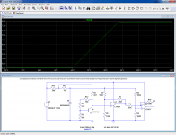
In the meantime, here is an (approximative) model of the circuit:
The soft-start and phase-control seem duplicate, and they probably are: it would be possible to coerce the phase control circuit into handling the soft-start function, but the phase-control was a later addition, and the soft-start was already present and operating properly, which is why I didn't remove it and simply added a supplementary layer.
In a version 2.0, this (and many other aspects) could certainly be streamlined.
The two Y capacitors, C22 and 23 probably look intriguing.
Strictly speaking, they are not needed: one could just reference the heatsink and the ferrite + its fastening bar to the primary 0V, which is where they belong, but I generally try to avoid the direct connection of large conductive parts to the live side: there is always the risk of a screwdriver or a probe slip, not even mentioning hand contact.
A Y cap ties the frames in question to the primary 0V for AC purposes, but avoids fireworks or worse in case of an accidental contact.
-
Secondary side:
The high voltage rectifier D1 has nothing remarkable except perhaps L13, which removes the effect of ringing on the output voltage: it is necessary to have a good convergence between the peak and rms output voltage to keep the heater and HV voltages in track.
For the servo section (previous schematic), this part is handled by R34, because only low power is involved, but for the main HV output, an inductor is required to limit the losses.
A varistor is present at the output to protect the capacitor.
The voltmeter module is a cheap 100V that has been modified to take 1000V: the decimal point has been zapped, and R4 increases the voltage range (the input resistance is ~100kΩ).
The 0 to -100V regulator section is more interesting, and can probably be reused for many other jobs:
The core of the regulator is Rush cascode (Q2 Q3) instead of the usual LTP.
Thanks to this topology, the input reference can go down to zero (below in fact), and so can the output.
The primary reference is provided by D5, which is in fact a 33V regulator IC intended for varicap voltage regulation.
It looks like an ordinary 400mW zener and behaves as a zener, but it has the stability and internal resistance of an integrated reference.
There are many alternatives like the TAA550 in metal case.
A TL431 could be used too.
Since the Rush has a 2*Vbe offset between the inputs, the voltage pot has its foot potential set by D8 and D9, which ideally should be plain vanilla silicon types, not gold-doped ones like the 1N914 or 1N4148.
The pass element is a N type, working in common-source, which means the regulator is a LDO.
I have added a simple overcurrent protection in the form of Q1, because it is part of a lab instrument.
The topology is highly scalable, from a few volts to a few hundreds volts (limited by the PNP member of the Rush), and it could easily be improved with minimal effort and investment.
I didn't go further, because the current circuit was perfectly sufficient for the purpose, but for a small standalone HV lab supply, some improvements in the regulation, reference and compensation are possible.
I will probably discuss these later.
In the meantime, here is an (approximative) model of the circuit:
Attachments
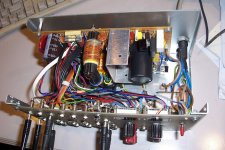
Fan controller:
I normally try to avoid fans, but I have included one in this project, more as an afterthought than by real necessity: when the total output power reaches 300W, some parts heat up significantly, mainly the transformer and the MOSFets heatsink.
Although the temperature rise remains safe, I felt more comfortable with a small, variable-speed fan: it remains inactive under normal circumstances, and only wakes up progressively when the sensor's temperature exceeds ~60°C.
The sensor is an E-line transistor slipped under the ferrite's clamping bar.
This location might look surprising, but it is in fact the most appropriate:
The transformer is designed with a large leakage inductance, thanks to separate secondary and primary windings.
When the load on the secondary is large (or in case of a short), it tends to block the magnetic flux generated by the primary. This flux is ejected from the transformer and baths its surroundings, inducing eddy currents into any metallic object happening to be in the vicinity.
The clamping bar being very close, and made of steel (a somewhat questionable design choice...), it is the first to heat up, and it does so very quickly thanks to its small thermal mass.
It is therefore the ideal place to sense the total power throughput.
A word about the fusing philosophy:
As I said earlier, fuses are the main protection means, except for the -100V regulator which has an electronic current limitation.
Every output is fused, including the winding taps, because any series or parallel combination is allowed, meaning an output could be taken between two taps and not only between a common and a tap.
The 2A fuses for the 0.5A HV windings look too large, and in fact they are: they are normally not supposed to blow.
What is the reason behind this apparent non-sense?
During the tests, I made sure the converter was able to blow any of the fuses when the corresponding output was shorted, but when I checked the 400V, I had a good fright: the fuse did blow as it should, but it didn't manage to interrupt the current: instead, a huge flame escaped and began to leach everything within reach.
Fortunately, I had the hand on the power switch in case things went wrong, and I was able to interrupt the fireworks before any damage was done.
Had this happened in real circumstances, with the box closed, it would have caused extensive damage.
The problem is that the high-voltage, high frequency AC is practically as bad as DC for contacts, fuses, etc: there is no interruption at the zero-crossings, and the plasma has no time to fade.
I concluded that the safest option was to never allow these fuses to blow: instead, I rely on the primary fuse, because the HV winding has a relatively high power, and this power is reflected at the primary.
The primary fuse sees only 160V, and blows perfectly safely.
Why didn't I simply replace the fuses by shorts? Because the individual taps represent a much lower power, and any inter-tap short might fail to blow the primary fuse, leading to transformer damage.
The 2A is high enough to allow selectivity between the primary and secondary fuses, but low enough to be safe for the windings
Attachments
For those interested, I now have put the concept to the test in a versatile and attractive 0-->500V, 0-->200mA lab supply.The 0 to -100V regulator section is more interesting, and can probably be reused for many other jobs:
The core of the regulator is Rush cascode (Q2 Q3) instead of the usual LTP.
Thanks to this topology, the input reference can go down to zero (below in fact), and so can the output.
The primary reference is provided by D5, which is in fact a 33V regulator IC intended for varicap voltage regulation.
It looks like an ordinary 400mW zener and behaves as a zener, but it has the stability and internal resistance of an integrated reference.
There are many alternatives like the TAA550 in metal case.
A TL431 could be used too.
Since the Rush has a 2*Vbe offset between the inputs, the voltage pot has its foot potential set by D8 and D9, which ideally should be plain vanilla silicon types, not gold-doped ones like the 1N914 or 1N4148.
The pass element is a N type, working in common-source, which means the regulator is a LDO.
I have added a simple overcurrent protection in the form of Q1, because it is part of a lab instrument.
The topology is highly scalable, from a few volts to a few hundreds volts (limited by the PNP member of the Rush), and it could easily be improved with minimal effort and investment.
I didn't go further, because the current circuit was perfectly sufficient for the purpose, but for a small standalone HV lab supply, some improvements in the regulation, reference and compensation are possible.
I will probably discuss these later.
It is rugged, based purely on commodity generic discretes, requires no auxiliary voltage, has a low drop-out (<1V), offers decent performances and can be dimensioned for a wide range of voltage/currents:
ELEKTR⚡A is a true High-Voltage lab supply, truly DIY-friendly
- Status
- This old topic is closed. If you want to reopen this topic, contact a moderator using the "Report Post" button.
- Home
- Amplifiers
- Tubes / Valves
- A "supply-center" for testing tube projects