Hi,
I've lived with this as a plate load for some while. Low capacitance and high impedance with the 'mu output' for low output impedance, whats not to like?.
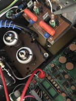
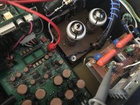
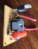
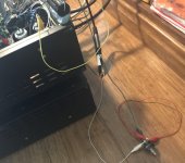
Have recently acquired a good Tek analog scope, and I'll let the pics tell the story. I constructed it using perfboard layout as close to the original PCB's and used the recommended parts. Yep, it sounds great.
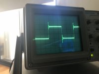
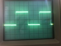
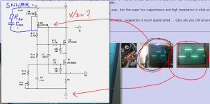
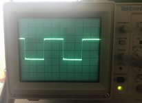
With mu output there is a voltage gain of 6dB at 500kHz, and square wave rings (at any frequency), screen shot is 1kHz.
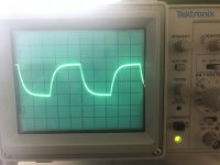
Taking output from the plate of the tube (at the 'bottom' of R1), all is clear up until well past 1.5MHz, the stage starts to roll HF off at a tick over 100kHz, and down by 6dB at 250kHz there abouts, no visible distortion of sine wave at all, until it rolls completely off well below 2MHz.
Any thoughts?.. buy a CCS kit that doesnt oscillate, yep.. but the super low capacitance and high impedance is what attracted me to this years ago. Could it be (and I'm not a SS guy), simply a matter of increasing the stopper to 100R or 1K in lieu of the 10R as specified.
Anyway, hope someone finds this useful and any information, suggestion is much appreciated. .. Gary are you still around??
Thanks.
I've lived with this as a plate load for some while. Low capacitance and high impedance with the 'mu output' for low output impedance, whats not to like?.
Have recently acquired a good Tek analog scope, and I'll let the pics tell the story. I constructed it using perfboard layout as close to the original PCB's and used the recommended parts. Yep, it sounds great.
With mu output there is a voltage gain of 6dB at 500kHz, and square wave rings (at any frequency), screen shot is 1kHz.
Taking output from the plate of the tube (at the 'bottom' of R1), all is clear up until well past 1.5MHz, the stage starts to roll HF off at a tick over 100kHz, and down by 6dB at 250kHz there abouts, no visible distortion of sine wave at all, until it rolls completely off well below 2MHz.
Any thoughts?.. buy a CCS kit that doesnt oscillate, yep.. but the super low capacitance and high impedance is what attracted me to this years ago. Could it be (and I'm not a SS guy), simply a matter of increasing the stopper to 100R or 1K in lieu of the 10R as specified.
Anyway, hope someone finds this useful and any information, suggestion is much appreciated. .. Gary are you still around??
Thanks.
Attachments
Last edited:
Thanks. Tried but to no avail.
I am looking for a replacement CCS, have emailed a few vendors, one of which replied that he had not tested his CCS (commercial off the shelf offering) beyond 100kHz, or at any stage with a square wave. (really?)
Failing a decent CCS, I'll spring for a 2:1 stepdown transformer, and just mount it to the back of the chassis.
Thanks.
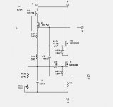
I would increase the value of R7 to some 680R, and as 2nd step decrease te 4k7. I do not know why Gary Pimm used such differing values (being gate stoppers) - still Rod Coleman posted recently that Gate stoppers should best be kept below 1k (for larger FETs even much lower than 1k)
Good luck! Erik
Good luck! Erik
With mu output there is a voltage gain of 6dB at 500kHz, and square wave rings (at any frequency), screen shot is 1kHz.
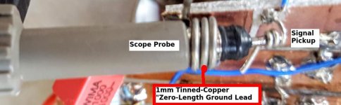
If you are measuring square waves from a low impedance source, the ringing you observe on the scope may be caused by the probing method, rather than a misbehaviour of the circuit.
The 'µ output' has a drive impedance of only a few ohms, and if the signal has a fast risetime, feeds a capacitive load, or has a large amplitude, the risk of coupling into the ground-lead of the probe increases, and can show ringing that will disappear with careful probing.
The easy thing to try is a 'zero-length ground lead' made from a length of 1mm solid copper (tin plated). Remove the probe's end-clip, and wrap the copper around the probe to form a tight coil. Then remove this coil and solder it to the ground-plane of the circuit under test. The picture tells the tale. This method prevents external fields from adding a [series] noise voltage in the scope probe return. As well as cleaning up square waves, the noise floor of the scope drops dramatically with this method.
I assume you're using x10 probing, and have trimmed the x10 probe for correct response, using the scope's squarewave generator.
Attachments
About the FET gate stoppers:
- depletion FETs. Usually, connecting the depletion FETs as current sources, even cascodes, means that the gate wiring can be very short, and the loop area around gate to source is correspondingly small. In this case, the danger of creating a Hartley oscillator (Drain wiring too long) or Colpitts oscillator (source-follower circuits) should not be too great.
Oscillation stems from coupling from drain to gate, and if the circuit wiring is well-implemented (easy with a depletion FET CCS), the coupling is mostly from the drain-gate capacitance. In this situation, a low gate-source impedance is helpful, since it suppresses signals arriving via this D-G capacitance. Adding a high-value gate stopper can allow the gate signals to increase, and this makes the oscillation worse - not the result we may have been expecting.
When the external gate wiring can't be made short (less than about 30mm) a stopper may be needed, but don't get carried away with the value. If the circuit is stable over a wide range of signal amplitudes using a 100Ω stopper, leave it at that.
In the circuit of post №1, the lack of stoppers for LND150 is probably fine, if there are no long wires leading to the gate(s). And Q1's 10Ω is also likely to be perfect, too, because the G→S circuit is suppressed by a large capacitor. Increasing the 10Ω may well lead to problems here.
The 4.7K in the gate of the other IRF820 seems too high to me, and this FET also sees very high impedance from gate to source. Noise pulses coupling through the D→G capacitance can prevent the channel from fully turning OFF, and the breakdown voltage may appear to be lowered. I wouldn't operate this circuit anywhere near the 500V rating of the IRF820.
The µ output has no series output resistor, which may be desirable for low output impedance, but the stability of the FET can be compromised by reactive loads acting as (example) an unintended Colpitts oscillator. If the system can stand some series resistance, a 50Ω resistor will help ensure stability.
Although this post by Gary relates to the Swenson/Pimm regulator it does give some important information on stoppers.
http://www.diyaudio.com/forums/tubes-valves/82641-look-voltage-regulator-projects-9.html#post1734963
Ale Moglia over at his excellent blog has posted his finding that sometimes the gate stopper needs reducing;not increasing.
And always follow Rod's advice.
tim
http://www.diyaudio.com/forums/tubes-valves/82641-look-voltage-regulator-projects-9.html#post1734963
Ale Moglia over at his excellent blog has posted his finding that sometimes the gate stopper needs reducing;not increasing.
And always follow Rod's advice.
tim
Thanks Rod, I will investigate this further.. really appreciate your comprehensive reply.
Also thanks to Tim, as this link provides some useful information as to why the values where selected;
R15, the resistor on Q2 is more than a just a gate stopper. It is actually tuning the speed of the MOSFET cascode circuit. If the value of R15 is too high, the circuit will oscillate in the 150Khz to 250Khz range with what looks like a relaxation oscillator. If the value of R15 is too low the circuit breaks into a chaotic high frequency oscillation that my Tektronix TDS460 scope can't trigger on well enough to get a frequency measurement.
This behavior has been constant with the CCSs, the amplifier modules, and the regulator circuit. The value is chosen to be at the approximate mid point between the 2 modes of oscillation.
In the self bias and battery bias CCS circuits when using the IRF820a parts the Q2 gate stopper was 2.2K. When the IRF820B came out the value had to be increased to 4.7K as the IRF820B is a faster part.
Last edited:
A too large gate resistor may have a diminishing effect as a gate stopper, R15 seems large.
Is C5 supposed to be connected to Q1 source, and what is the value of R1?
Also, as already mentioned, probes themselves can interact with the circuit and one thing you could try out is attaching something like a 1k resistor in series with the probe tip.
Is C5 supposed to be connected to Q1 source, and what is the value of R1?
Also, as already mentioned, probes themselves can interact with the circuit and one thing you could try out is attaching something like a 1k resistor in series with the probe tip.
Last edited:
The reasoning behind the value for R15 gate resistor is given by the designer of the cct as indicated above.
I do not know where C5 could otherwise be connected, the guy who designed it was an engineer who worked for Tektronix - I went with the schematic.
Will also try the 1k series resistor as you suggest and report back.
R1 = 1k2.
Thank you.
I do not know where C5 could otherwise be connected, the guy who designed it was an engineer who worked for Tektronix - I went with the schematic.
Will also try the 1k series resistor as you suggest and report back.
R1 = 1k2.
Thank you.
Last edited:
Yes, you can try the 1K with the probe, but if you have a x10 probe, there should be no need. The µ output should not be sensitive to a few pF of capacitance.
The experimentally determined value of the gate resistor may work reliably for a reasonable range of parts, but beware that the IRF820 is almost generic - available from ON, ST, Vishay/siliconix,as well as the IR original. It could turn out that the processes have changed since the article was written, or that some vendor's parts have different capacitances, gm etc. and that this compensation method is not guaranteed to work.
If it really oscillates at 200kHz, even with cleaned-up probing, the effect is not self-oscillation of the FET, but an unintended oscillator composed of several different components. This kind of problem can almost always be fixed in a reliable way, without compromising the gate stoppers.
OTOH, Ale's 'gyrator' boards should be able to host an equivalent to this anode-load circuit, and has been tried by plenty of constructors. It's probably easier to get a set of these, that try to debug a circuit like this.
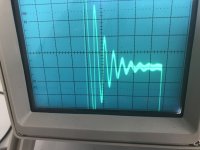
Looks more like overshoot that rings... And if fine on the tube's plate, and sounds good...?
The ringing (overshoot) is the same independent of frequency b/c it is the fast edge and not the frequency that causes the ringing. Does it ever get a fast edge signal under normal use?
Anyways when probing high frequencies, fast edges have very high frequencies, you must have a very small loop on the probing.
I have a very similar circuit used as a stepped/pulsed load to test power supplies, and it oscillated when I came over some current level. Tried all sorts of gate resistances etc, layout is tight. Ended up with a snubber over the load MOSFET (IRFB11N50) and all is good. I used 1n and 22ohms, didnt spend time optimising, I just got it working and happy.
Perhaps a snubber will help damp out your ringing from the overshoot?
Oh and am I correct with where your square waves are measured?
Attachments
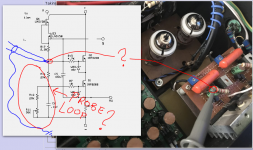
Thanks. Fast edge with normal use, well.. no, but there is quite substancial voltage gain increase at ~550kHz with a sinewave of any amplitude.
The two scope shots are taken at either end of R1 in the schematic wrt ground, and no.. not the shortest loop and on x1 and not x10 and without any series resistance etc (yet). I did think about just taking the output from the tube plate and be done with it, but combination of mild OCD and that I am wanting to use the 'mu output' for lower output impedance is enough to keep me interested in sorting this out .If indeed it turns out to be a probing issue, or requiring some adjustment to the gate stopper based on production inconsistencies as suggested above, I'll be happy.
Just need to find the time now.
Last edited:
Would you believe it..
My nice square wave was taken with the load disconnected (a flurry of twenty different actions all on a whim). And the load is... an AVC, and the secondary of that AVC is .. essentially unloaded, 1M.
I start looking around and I find this excerpt which looks very familiar to me (http://jensen-transformers.com/wp-content/uploads/2014/09/Audio-Transformers-Chapter.pdf)
My thinking was based on what I believe to be a misunderstanding that I was wanting lowest drive impedance, highest load impedance and the smallest sized coupling capacitor to fit the LF requirements.
I think to keep the CCS load, take the output from the plate of the tube to increase slightly the drive impedance to ~2kohm, and load the AVC by reducing amplifier input impedance from 1M to 100k.
Stevens & Billington Limited Audio transformers TX-102
Thanks to all for advice and suggestions, hopefully you can see the funny side of it. The waveform in the excerpt is identical.. and my apologies to Mr Pimm for any suggestion that his CCS was the issue here.
Attachments
Last edited:
Just to follow up;
Changing the load across the autoformer from 1M to 100k made no change to the square wave response.
Adding an RC across the autoformer (with the 100k load still in place) squared things up and rolled of the HF response accordingly. The only values which really worked were 10nF+33R, 4700pF+8R2, or straight out 56nF without series resistance. I removed them.
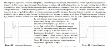
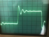
Adding series resistance from the mu output allowed to damp the ringing (Image 5) and without visible distortion to over 200kHz where it started to roll-off, and of course no huge amplitude peaks between 500 and 600kHz.
Taking the output from the D3a plate provided square wave response as shown in (Image 6), no visible sine wave distortion but started rolling off gradually at 15kHz.
Value of series resistance as determined by rheostat was 190ohm. Not sure if it matters whether this is before or after the output coupling capacitor.
I did stumble across this; Electra-Print.com Tech Blog but for the cost of two resistors and response without ringing out to 200kHz, I'm ok with the resistors.
Changing the load across the autoformer from 1M to 100k made no change to the square wave response.
Adding an RC across the autoformer (with the 100k load still in place) squared things up and rolled of the HF response accordingly. The only values which really worked were 10nF+33R, 4700pF+8R2, or straight out 56nF without series resistance. I removed them.
Adding series resistance from the mu output allowed to damp the ringing (Image 5) and without visible distortion to over 200kHz where it started to roll-off, and of course no huge amplitude peaks between 500 and 600kHz.
Taking the output from the D3a plate provided square wave response as shown in (Image 6), no visible sine wave distortion but started rolling off gradually at 15kHz.
Value of series resistance as determined by rheostat was 190ohm. Not sure if it matters whether this is before or after the output coupling capacitor.
I did stumble across this; Electra-Print.com Tech Blog but for the cost of two resistors and response without ringing out to 200kHz, I'm ok with the resistors.
Attachments
Reviving this thread as I have a couple questions about the Pimm self-biased CCS. I'm interested in using it as a plate load for my UX-201A preamp, to compare it to the mu-output K&K CCS I'm using now, but it is not easy to find detailed information about the parts used.
1) In the schematic in the first post of this thread the 100uF cap is shown with the symbol for a non-polar electrolytic, yet in pictures of the assembled board I think I can see a black stripe down one side of the cap, indicating the negative. Is that cap polar or non-polar?
2) Also, for the same cap, what voltage rating did you use? I have some polar 350V caps I could use, which is likely overkill on the rating.
I will be using the AOT1N60 MOSFET in place of the IRF820B. I originally bought several of them for my 833C amp but instead used its big brother, the AOT2N60 and have been very happy with its performance. It has MUCH lower capacitance than the IRF820B which is obsolete and has become very hard to find.
Any help is greatly appreciated!
I have some polar 350V caps I could use, which is likely overkill on the rating.

and then some
- Home
- Amplifiers
- Tubes / Valves
- Gary Pimm self bias CCS 500kHz 'ringing'