
Hey guys...
In the sim I did, I found that the 7591's really misbehaved if they didn't have screen stoppers of at least 1k ohms. What's the downside to using screen grid stoppers of a higher value than needed?
I did a mock-up, mostly to satisfy my own curiosity. It doesn't have the combination-bias.
When adding NFB, the low frequency cutoffs create a problem where the input/driver tube tries to add back the bass it sees at its input through negative feedback. This can cause the input tube to overload, or at least distort more than it should. I see that there's an input blocking cap for the El Cheapo.
I went in a different direction, using 1uF interstage coupling caps and 1000uF cathode bypass caps for the 7591's. That's easier to do in a spice sim than in real life, of course. Large value parts are both large in size and don't often perform as well as smaller value caps.
By the EH 7591's being "intolerant of violations of the published grid to ground to ground resistance limit," did you mean that they need a smaller value than the published specs, in order to keep from drawing grid current? My experimental circuit has the 7591's cathode biased, and with 470k ohm grid leak resistors, which is half the spec sheet maximum value.
At any rate, for what it's worth, and for curiosity's sake only, I've attached what I whipped up earlier.
Attachments
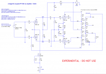
The interlocking circles are the symbol for a constant current sink/source (CCS). In this setup, it's a 6 mA. sink that connects to B-. The carbon film resistor between the 'T7 cathodes and the CCS is there to thermally isolate the "sand" from tube generated heat. Depending on the voltage of the C- supply, that part can, and probably will, become 100 Ω. Label the "flapping" side of the CCS as to B-.
The 7591 control grid stoppers should be 10 K carbon composition parts, not 100 Ω carbon film. Carbon comp. parts make good control grid stoppers because they are both non-metallic and non-inductive. Using 10 K mates well with the 7591s high gm and provides some help with a phenomenon called blocking distortion.
100 Ω/1 W. carbon film parts as the 7591 screen grid resistors is fine.
The 330 K 7591 grid resistors don't connect to the bias network. Label the junction of the 330 K resistors as to C-. The end of the RC bias network not connected to the 7591 cathodes is grounded. When assembly is complete, you will measure the voltage drop across the 100 Ω resistor, while adjusting the bias set trim potentiometer. The 7591 data sheet suggests that the drop will be approx. 8 V. The final value will be affected by the exact B+ rail voltage obtained.
Last edited:

By the EH 7591's being "intolerant of violations of the published grid to ground to ground resistance limit," did you mean that they need a smaller value than the published specs, in order to keep from drawing grid current? My experimental circuit has the 7591's cathode biased, and with 470k ohm grid leak resistors, which is half the spec sheet maximum value.
"Fireworks" have been reported in Fisher units, where the OEM grid resistor is above the 300 K allowed for "fixed" bias. Add in age related upward drift in a carbon comp. part.
 1 Mohm is the limit for self (cathode) bias. Employing combination bias allows for a small liberty to be safely taken. If a tube starts "running away", the increased cathode current causes the voltage drop across the 100 Ω resistor to increase and the excess current is driven down towards the intended value. It's a very simple servo mechanism and is why grid to ground limits are higher for cathode bias than they are for "fixed" bias. I don't want to over rely on the mechanism, when only 8 or so V. of the total bias is self generated by the PP pair.
In the sim I did, I found that the 7591's really misbehaved if they didn't have screen stoppers of at least 1k ohms. What's the downside to using screen grid stoppers of a higher value than needed?
What sort of bad behavior did you observe? Using a 1 K 7591 screen grid resistor will limit g2's contribution to the total power O/P, but will not (AFAIK) create any real problem.
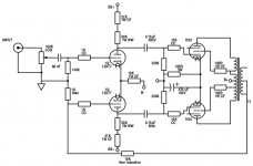
Like so?
Btw sorry about the transformer, could not find a sample with enough secondaries.
Still trying to figure out what to use to make schematics
It's getting there.
")
7591 B+ is "taller" than 'AQ5 B+. So, the total 'T7 section load resistance can increase. Add 1 W./27 Kohm carbon film parts between the 50 Kohm wirewound parts and B2+. "Ordinary", inductive, WW resistors are intentionally used to cause a bit of HF "peaking". However too much HF boost will be counter productive. Boosting HF compensates for the rolloff in O/P "iron" of modest cost. We hope to get the closed loop HF 3 dB. down point near 80 KHz. A very large NFB generated HF error correction signal could induce slew limiting.
So, we add some HF boost in the driver to compensate for the O/P trafo's natural behavior and rely on NFB to finish things up, rather than "the whole enchilada".BTW, I hand draw schematics and they look like hen scratches.
What sort of bad behavior did you observe? Using a 1 K 7591 screen grid resistor will limit g2's contribution to the total power O/P, but will not (AFAIK) create any real problem.
I've found that if processing suddenly takes an inordinate length of time, that usually means LTspice is computing something strange, which might be a predicted oscillation or other such anomaly. I couldn't wait for the sim to complete, so I canceled it and changed the 100R screen grid stoppers to 1k. After that, the simulation ran as expected. I took that to mean that LTspice had found some sort of problem. Then again, it could mean nothing more than some quirk in the program, or possibly in the tube models I'm using.
I once tried 'mixed bias' on a guitar amp, with 6L6's. It worked great, and sounded really good. Clipping behavior was very smooth and well controlled (important for a guitar amp).
What you mean "taller"?
I added it!
In the 'AQ5 amp, B+ is (ideally) about 355 V. The 7591 amp's B+ is above 400 V. The 'T7 triode sounds good with 3 mA. of plate current and 200 to 220 V. on the plate. In order for the voltage on the 'T7 plates to be correct, additional resistance is needed between those plates and the B2+ rail. The added resistance works to our advantage in compensating for the reduced O/P tube grid to ground resistance. Remember, gain is function of AC impedance and the plate load resistance and grid to ground resistance are in parallel, from an AC perspective.
The O/P tube grid biasing error is back.
Only the RC bias network is grounded. The junction of the 330 K resistors connects to C-, not directly to ground.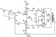
Sebastian,
The schematic is shaping up, but still needs some work.
The volume control is 10 K, not 100 K. Remember the 1:10 driver/driven impedance ratio rule.
The LTP's tail CCS has been omitted. Insert a 6 mA. CCS between the thermal isolating resistor and B-.
Speaking of the CCS, the original "El Cheapo" schematic shows a cascoded FET setup. However, any high quality CCS setup will work. IIRC, some European members have PCBs for a cascoded BJT setup. It may be logistically and financially more convenient to hunt that down.
Luckily I am able to buy DN2540N5s from Hungary, and will use them. I will correct my faults tomorrow. One more question I have: Do I have to make one CCS for the 2 channel, or I have to make one for one channel and one for the other?
What is input B- voltage?
Sorry about the questions, but I really want to understand what I do, not just copy and paste your work
Edit: Although I don't know the Voltage, I should ask: Will I have to apply heatsink on the DN2540N5s?
What is input B- voltage?
Sorry about the questions, but I really want to understand what I do, not just copy and paste your work
Edit: Although I don't know the Voltage, I should ask: Will I have to apply heatsink on the DN2540N5s?
Last edited:
We'll have to see how B- works out. Each channel gets its own CCS. At 6 mA. in each channel, heat sinking of TO220 case FETs seems unnecessary. At worst, small clip on parts will be needed. Make sure you build with good air circulation.
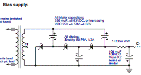
I'm uploading a schematic for a voltage multiplied C- (bias) supply. While you will not exactly replicate it, the 1/2 wave parallel topology shown will get used. A nice feature of that sort of setup is the ability to take off more than 1 voltage and this project needs 2 different negative voltages.
I'm uploading a schematic for a voltage multiplied C- (bias) supply. While you will not exactly replicate it, the 1/2 wave parallel topology shown will get used.
A nice feature of that sort of setup is the ability to take off more than 1 voltage and this project needs 2 different negative voltages. Attachments
Obisix,
Entering this late, I am really glad you are getting it right. In the beginning I shared your 'anguish'; many people will provide you with many options based on personal preference, leaving you none the wiser. As I read along I am glad that you rather went for some 30W (with the possibility of going still higher). I cannot compare on the basis of cost at all as in South Africa the situation is quite different from yours. I would also have advised begging/borrowing/stealing (er - well, perhaps not the latter) to get something which could serve you for some time. This thread is a valuable lesson for all desiring to go this way; all credit to Eli for patience.
If you will allow some space to make a side comment to Ron:
Ron,
Eli already suggested why. Another factor is that G2 draws current, thus input thataway is into a finite impedance, not the usual high impedance grid situation. The UL advantage can be compromised by too a high a g2-resistor. I know the exception is with the EL34; this is a subject for a different thread.
I would agree that your simulation program may have tried to 'close' on a minute detail; I have never found instability as a result of a too low g2-resistor. Respectfully, skeptical as to how close-to-reality UL transformer Spice models are.
Back to topic: Good luck Sebastian, further patience will be needed when you start constructing! But stick with it; we all came that way (you will laugh at how long it took me to understand the difference between voltage and current many decades ago!) As Eli did I will encourage you to read up. Google is your friend; so much good information there. (When I started we could not spell 'Google' or 'computer'; had to do with books and magazines ....)
Regards,
Johan
Entering this late, I am really glad you are getting it right. In the beginning I shared your 'anguish'; many people will provide you with many options based on personal preference, leaving you none the wiser. As I read along I am glad that you rather went for some 30W (with the possibility of going still higher). I cannot compare on the basis of cost at all as in South Africa the situation is quite different from yours. I would also have advised begging/borrowing/stealing (er - well, perhaps not the latter) to get something which could serve you for some time. This thread is a valuable lesson for all desiring to go this way; all credit to Eli for patience.
If you will allow some space to make a side comment to Ron:
Hey guys...
In the sim I did, I found that the 7591's really misbehaved if they didn't have screen stoppers of at least 1k ohms. What's the downside to using screen grid stoppers of a higher value than needed?
Ron,
Eli already suggested why. Another factor is that G2 draws current, thus input thataway is into a finite impedance, not the usual high impedance grid situation. The UL advantage can be compromised by too a high a g2-resistor. I know the exception is with the EL34; this is a subject for a different thread.
I would agree that your simulation program may have tried to 'close' on a minute detail; I have never found instability as a result of a too low g2-resistor. Respectfully, skeptical as to how close-to-reality UL transformer Spice models are.
Back to topic: Good luck Sebastian, further patience will be needed when you start constructing! But stick with it; we all came that way (you will laugh at how long it took me to understand the difference between voltage and current many decades ago!) As Eli did I will encourage you to read up. Google is your friend; so much good information there. (When I started we could not spell 'Google' or 'computer'; had to do with books and magazines ....)
Regards,
Johan
Sebatian,
Yes, each channel's LTP tail CCS gets adjusted to pass 6 mA.
Strategically placed holes that allow convection currents to move heat are, in general, a good idea. Look at the photos of builds, both here and over on AA. Quite a few have ventilating holes.
Johan,
Thanks for the vote of confidence in 100 Ω 7591 g2 resistors. I want to protect those screen grids from excessive dissipation, while not interfering with UL mode's local NFB.
All,
I think I've come up with a near perfect power trafo for this project. It's the AnTek AS-3T325. That "puppy" will definitely get the B+ rail above 400 V., even after allowing for the inevitable losses real world projects exhibit. Somewhat above 400 V. for B+ is (IMO) "ideal". With over 400 mA. of B+ current available, transient performance should be excellent. I like reserves of current.
Well I made the CCS schematic you provided Eli, also I corrected the errors I made with the El Cheapo schematic.
I'm still reading how to design a BJT CCS, and will post that too when I figure it out, but until then, I steal your work.
Any corrections?
Thank you Jonan, will use your advises! I'm really happy too that Eli helps me!
I'm still reading how to design a BJT CCS, and will post that too when I figure it out, but until then, I steal your work.
Any corrections?
Thank you Jonan, will use your advises! I'm really happy too that Eli helps me!
Attachments

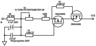
Credit for the CCS goes to Doug Piccard, AKA Bandersnatch, not me. The 100 Ω resistor between the FET cascode and the current set trim pot. is a 1 % tolerance part of low wattage. When 6 mA. are passed through 100 Ω, all of 0.0036 W. are dissipated. That part is the test point. The 10 turn pot. is adjusted to get a 0.6 V. drop across the 100 Ω. The 5 K resistor and 2 caps. are really part of the B- rail filter, not the CCS proper. Those values are subject to change, as we work the negative supplies voltage multiplier out. The thermal isolator CF part between CCS and tube socket is subject to a value change too, for the same reason.
Approx. 30 V. are needed to operate the CCS. Additional volts are needed to provide LTP "compliance".
That part is the test point. The 10 turn pot. is adjusted to get a 0.6 V. drop across the 100 Ω. The 5 K resistor and 2 caps. are really part of the B- rail filter, not the CCS proper. Those values are subject to change, as we work the negative supplies voltage multiplier out. The thermal isolator CF part between CCS and tube socket is subject to a value change too, for the same reason.Approx. 30 V. are needed to operate the CCS. Additional volts are needed to provide LTP "compliance".
- Home
- Amplifiers
- Tubes / Valves
- Choosing a tube amplifier to build, HELP needed