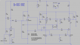
Hi George, or anyone else willing to look at my simulation.
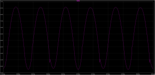
I tried simulating your posted circuit and get horrific distortion (5713.491356%) at 1.6Vrms out.
The .sub and .inc files won't attach so here are the lists:
****
*
* R McLean 24 June 2005
* combine best features of Duncan Amps and Korens version
* 6AU6 pentode
* parameter extraction, from GE tube sn001, 24 June 2005
****
*
.SUBCKT 6AU6 A S G K
+ PARAMS: Ex=1.29250482718994 Kg1=1066.05313830636 Kp=233.038097126617 Kvb=6.26797667003452 Mu=39.2114621352395
+ Exd=0.927382241593347 Kd=1427.5732907893 Ks=2.80629495414095 Kg=0.00189539610643784
+ CCG=5.5P CPG1=.0035P CCP=5.0P
Eat at 0 Value={limit(0.636*ATAN(V(A,K)/KVB),0,1)} ; arctangent shaping
Eme me 0 VALUE={PWR(LIMIT(V(A,K),0,2000),EXD)/KD} ; diode line
Egs gs 0 VALUE= {V(S,K)/KP*LOG(1+EXP((1/MU+V(G,K)/V(S,K))*KP))} ; effective voltage
Egs2 gs2 0 VALUE={(PWR(V(gs),EX)+PWRS(V(gs),EX))/(KG1*0.636)} ; total space current
G1 A K VALUE={LIMIT(V(gs2)*V(at),0,V(me))} ; plate current
Escrn sc 0 VALUE={KS*V(gs2)*(1.1-V(at))} ; reverse arctan shaping for screen current
G2 S K VALUE={V(sc)*LIMIT(V(S,K),0,10)/10} ; screen current
G3 G K VALUE={PWR(LIMIT(V(G,K)+1,0,1E6),1.5)*(1.25-V(at))*KG} ; grid current
C1 G K {CCG} ; CATHODE-GRID 1
C2 A G {CPG1} ; GRID 1-PLATE
C3 A K {CCP} ; CATHODE-PLATE
.ENDS 6AU6
*Vacuum Tube Tetrode (Audio freq.)
.SUBCKT X50C5 A S G K
*
* Calculate contribution to cathode current
*
*the number at the right end determines sharpness of knee
Bat at 0 V=0.636*ATAN(V(A,K)/12)
*the URAMP(V(S,K)/# mostly determines peak plate current, grid line spacing nearly constant
*the number at the right end determines slope of grid lines
Bgs gs 0 V=URAMP(V(S,K)/6.2+V(G,K)+V(A,K)/90)
*the exponent sets the linearity of grid line spacing, and big impact on peak plate currrent
Bgs2 gs2 0 V=V(gs)**1.58
Bcath cc 0 V=V(gs2)*V(at)
*
* Calculate anode current, grid line spacing adjust and peak plate current
*
Ba A K I=1.35E-3*V(cc)
*
* Calculate screen current
*
Bscrn sc 0 V=V(gs2)*(1.1-V(at))
Bs S K I=0.6E-3*V(sc)
*
* Grid current (approximation - does not model low va/vs)
*
Bg G K I=(URAMP(V(G,K)+1)**1.5)*50E-6
*
* Capacitances
*
Cg1 G K 13p
Cak A K 8.5p
Cg1a G A 0.6p
.ENDS X50C5
Attachments
Hi George, or anyone else willing to look at my simulation.
I tried simulating your posted circuit and get horrific distortion (5713.491356%) at 1.6Vrms out.
Maybe the distortion to the output waveform might suggest something. Apart form the obvious glitches the positive excursion is greater than the negative excursion.
I tried disconnecting the feedback to the screen of U1 while duplicating it's biasing but that didn't help.
Attachments
Reverse polarity of L3.I tried simulating your posted circuit and get horrific distortion (5713.491356%) at 1.6Vrms out.
I managed to modify and tweak the circuit for the 6P1P-EV.
>30W at 10% THD!
The tubes are running at 85% max dissipation (12W).
IT will probably take me a while to test this, but I really look forward to it.
I had a number of issues with LTSpice reporting step size errors and had to isolate the screen supply to the input tube.
I also switched to the 6CB6 as the input tube as I have a nice supply of them.
Attachments
In the circuit you are simulating the grid is not grounded. Negative feedback via a resistor directly from the plate of the tube makes the pentode look a lot like a triode. This was discovered by Schade back around 1940, but always involved at least one capacitor in the path.
Now that you have your sim running put a probe on the cathode and control grid of an output tube. All will be moving in phase, but at different levels. The only element that's not moving is G2. So the drive is directly applied between G2 and the cathode while the drive minus the local negative feedback is applied between G1 and the cathode.
Using this arrangement has several advantages.
No negative voltage supply is needed.
The total output stage dissipation is split between the tube and the mosfet. The ratio of this split is dependent on the idle voltage on G1.
At idle the tube sees a voltage on its cathode as in cathode bias, but this voltage is not wasted in a resistor as when driven to full conduction the cathode voltage is near zero putting all the B+ to work driving the OPT.
The "triodness" of a given pentode can be adjusted by changing the amount of feedback from the plate. This can be done easily with a large cap and a variable resistance from G1 to ground, also offering a low frequency rolloff. For those who prefer not to stick a big cap here, one can switch different plate to grid resistors, while also switching a resistor from G1 to B+ to result in the same voltage on G1. I have a small tube version working with a 6 position switch to go from triode like curves, to full pentode.
This concept can be used with true sweep tubes that need G2 around 150 volts. It can also be used with the common audio tubes with G2 at a higher voltage. The G2 supply is the only thing that needs to be changed.
The same concept can be used to reduce the effective Mu of a triode. I have made it work in simulation with those high Mu regulator beam triodes, but the first test in a real circuit blew up in an oscillatory fashion as those tubes are prone to do. Mu=300 Gm=65000 very hard to tame!
Disadvantage, all signals are in phase! care must be used in layout, and decoupling is likely needed on power supply lines even in a two stage amp.
Last edited:
Thanks George. I should have realized this as I noted the in phase relationship of the grid and cathode. And while adjusting the plate to grid feedback noted it's impact of the spectrum of harmonics.
I have an SE version of this simulating now using a 6P41S that looks like it can hit 17W at 10% THD but third dominates above 1W. If I increase the feedback to get more triode like behavior I can still get over 10W at 10% THD.
Pretty amazing circuit.
I have an SE version of this simulating now using a 6P41S that looks like it can hit 17W at 10% THD but third dominates above 1W. If I increase the feedback to get more triode like behavior I can still get over 10W at 10% THD.
Pretty amazing circuit.
I saw a 36LW6 hit 40 watts at 3% THD back in post #31 when fed with a certain BIG A$$ HP power supply set on 600 volts. The same board wired up as a single push pull amp has been to over 300 watts.
I am now trying to curve trace a couple 36LW6's and 26HU5's without blowing them up. I am still tinkering with this design. Despite working on this off and on for nearly 10 years, there is still more to learn about it.
I am now trying to curve trace a couple 36LW6's and 26HU5's without blowing them up. I am still tinkering with this design. Despite working on this off and on for nearly 10 years, there is still more to learn about it.
Question George. Is there anything in particular we should look out for when choosing P-FETs besides SOA?
I am looking at using the TP0610T (multiple vendors, I don't know which I have) for the front end P-FET. It looks very similar to the BSS84 for Rdson, capacitance, breakdown, etc.
The big issue with the FET under the output tube is SOA, no? Along with low capacitance, and Vds with margin for drive voltage peak.
I guess that I should have made it clear that I don't always use the same part in my circuits that's in the simulation. I stuck the first part that LTspice had in it's library that looked like it would work into my sim. If it worked, I left it in the sim.
Once the sim was working, I put the characteristics that I wanted for that sim into Digikey's web site, picked out a page or two full of suitable parts with the right package, sorted by price, and bought 5 or so of each. The actual part I have been using in my input stages for everything from the 50C5 amp to the 250 watt 36LW6 monster is the Microchip VP0106 in a TO-92 package. Anything similar in a breadboard / PC board friendly package should work.
The phase inverter in the 50C5 amp is a Microchip LND150 in TO-92, and the output stage gets a Fairchild / ON Semi FQP3P50. There are probably better choices than the 3P50 in that output stage, but I had a bunch and they worked.
The big powered amp gets Fairchild FQPF9P25's since they are the only part that I haven't blown up, and you know how big my power supply is. Bad stuff happens when it gets hungry, especially when running at full crank. Yes, SOA is the big thing here, followed by the usual Crss and Gm. I pick a Vds spec with some margin above the voltage needed to fully cutoff the output tube under the expected operating conditions, and current capabilities beyond what the tube should handle.
It's the linear region SOA in between the extremes that's tricky, and poorly specified by the mosfet vendors, especially Fairchild/ONSemi. Beware of ANY mosfet where the DC SOA rating is equal to the rated dissipation, or a mosfet with no DC line on the graph. Secondary breakdown in mosfets wasn't well understood when I left Motorola in 2014, many vendors still believed that it didn't exist.
Is secondary breakdown a localized (on/within the die) thermal runaway? I was reading an application note from Toshiba and a Wikipedia entry, trying to understand a little. As mosfet temp increases the resistance decreases? Toshiba data sheet below.
https://www.google.com/url?sa=t&rct...sp?did=63593&usg=AOvVaw3j81IIyMgpkKTWWvj7yB3p

https://www.google.com/url?sa=t&rct...sp?did=63593&usg=AOvVaw3j81IIyMgpkKTWWvj7yB3p
Thanks George.
Interesting that the VP0106 is available in TO220, TO39, TO52, and TO92. I have them in the TO220 package.
I will probably try the TP0610T for the input tube. I have plenty in SOT23 and have adapter PCBs for them to go to through hole.
I don't have any FQPF9P25, but I do have a FQP3P50. It looks like they would be robust enough for my application. I do not plan on testing big sweep tubes.
I am considering purchasing a 1' section of 5" dia lexan pipe to place over the output tube during the test.
Are you using your big HP power supply for testing this stuff?
I place inverted coffee mugs over the mosfets on my line powered SMPS experiments.
I did have one 6HJ5 shatter, and another explode. Granted that these were being tested with the big HP turned up to 600 volts. A dumb math error led me to attempt to pass a 1/2 Amp pulse through the tube / mosfet combination at which point it all blew up, shattering the bottom of the tube.
How DUMM was that? Not as DUMM as trying it again expecting a different result. This time the tube exploded scattering glass all over the bench and floor. So, 600 volts times 1/2 amp is how many watts????? Even a dumm blonde should have realized this before pushing the button, but NOOOO, I had to do it twice!
I guess it didn't seem too far fetched since I actually tested a 6LW6 to higher power levels than this. Note the green line in this plot goes to 650 volts at 930 mA. That tube is still alive and well two years later.
The initial short circuit current on those power supplies is very large since there is 1000uf of capacitance across the output inside the supply, capable of delivering over 200 joules of energy to any unsuspecting part. I'm still not sure which blew first, the tube or mosfet since there was not much left of either. I'm setting up to curve trace some more big tubes. This time I will put my two big 8 ohm 500 watt resistors in series with the test subject to limit the explosions to minor levels.
Attachments

Hi George,
Yes, I am using the HP supply but don't expect to go north of 450V. I was thinking the same thing about putting some limiting resistance in series with the PS in case of a failure. Even at 450V that is a lot of stored energy, just over 100joules.
I went ahead and ordered the Lexan pipe to use as a shield, and will come up with something to cover the FETs as well.
I wonder if this 600V fuse would be worth inserting on the output of the PS.
https://www.allfuses.com/pub/media/documents/Littelfuse%20KLKD.pdf
Last edited:
- Home
- More Vendors...
- Tubelab
- UNSET is coming?