The board pictured throughout this thread is available as stated in post #29. I got them made in 2015 and moved before ever opening the box.
I fired one pair up in late 2016 when I was building my new lab, but got derailed and never got back to them until late 2017. That post caused all 32 remaining boards to disappear, so I got another batch made. There are about 55 of them left, and they are available for order.
What's not available is a full detailed set of build instructions. I have some other commitments that will keep me busy for the next couple of months, so not much new info will be coming from me. If you feel that you can build something from the info in this thread, then order them.
I will get a set of full instructions for this board and the new TSE-II up on the web site as soon as I get free to make them.
Mouser prompts FDP5N60NZ as a substitute for the obsolete NDF04N60Z. Is this acceptable?
Looks like the same characteristics both ways. but one is either easier to make or cheaper. May be rohs issues too.
https://www.onsemi.com/pub/Collateral/NDF04N60Z-D.PDF
https://www.onsemi.com/pub/Collateral/FDP5N60NZ-D.pdf
Hi George, thanks for your research time and effort. I have two types of European valves, E130L and RS1003, I got many of each in my time of living here. I am intrigued in use your AB2 with this valves, one is a sweep and the other is a transmission one, but both behavioured similar, different G2 lower voltage than Anode, anyway I planned in use they as triode, with no much power but linearity. Profiting the extra kick of grid current or 2. Do you think is possible in obtain a good result with your new AB2 circuit?
I travel to Florida cause my Mom will be 80 at the end of this month and I want to get a couple of drivers from you and any extra gadget for SE you have. Do you still live in Florida as I saw before on the past?
Best Regards and congratulations for your effort sharing your findings between this community of freaks.
Do you still live in Florida as I saw before on the past?
No. I packed up and moved everything about 1200 miles north when my 41 year career at the Motorola plant in Fort Lauderdale came to an end. That was over 5 years ago.
I have two types of European valves, E130L and RS1003
I don't know the RS1003, but I do have a box full of E130L's and they are nice tubes. I played with them a lot when i got them years ago, but they are still in the box for now....I'll get back to them someday.
Feedback
I'm interested in trying feedback in my UDB, KT-88 mono amps. George's post 311 (above) and Gimp's schematic in post 313 are pretty specific, but I still have a couple of questions. First, I'm confused as to the connection point at the OPT (or speaker terminal). Second, is the referenced 4k-10k resistor at the OPT connection point? Finally, Am I correct in assuming the small cap would be something like a 100v ceramic?
Any guidance here would be appreciated.
Thanks,
No, lift the ground end of C1 out of the board and wire a 100 ohm resistor in series with the cap. The resistor goes between the ground hole in the board and the lead on the capacitor that you just pulled out of that hole. Then inject the feedback into the junction of the cap and resistor. This is done with as resistor in the 4000 to 10,000 ohm range from the speaker terminal. Most OPT's will also work better with a small cap across this resistor.
If a phasing issue causes the amp to oscillate, swap the plate leads on the OPT.
I'm interested in trying feedback in my UDB, KT-88 mono amps. George's post 311 (above) and Gimp's schematic in post 313 are pretty specific, but I still have a couple of questions. First, I'm confused as to the connection point at the OPT (or speaker terminal). Second, is the referenced 4k-10k resistor at the OPT connection point? Finally, Am I correct in assuming the small cap would be something like a 100v ceramic?
Any guidance here would be appreciated.
Thanks,
One side of your OPT is grounded. Connect the 4-10K resistor from the other terminal to the junction of the 100Ohm resistor and cap in post 311.
The small cap is placed across the 4-10K resistor. It should be a silver mica cap or PolyPropalyne in the 50-1500pf range, at least 50V, but Silver mica are usually several hundred volt rated.
If you have an oscilloscope, inject a 1KHz square wave signal in your input and monitor the output of the amp. Try different values of capacitance to minimize the overshoot and ringing on the square wave.
Hi George, thanks for your effort, I was in the USA and acquired a set of boards both TSEII, pushpull and Universal driver. A set for another member of Slovenia to which I sent them after we bought them together.
All good, the boards very well finished and referenced. Thick and with a generous copper layer. Then I packed them and brought them to Spain.
Here as I said I want to build an AB2 prototype and try RS1003 and E130L. I did not have many references in the precise instructions concerning the supply voltages of the board, at the end after reading all the thread, I knew it was +150 -150volt.
I was seeing the schematic and it is the condensation of all the solutions that I had imagined with my mind, something narrow but pretentious. I think the thing can make it work well.
But I have some questions which can be answered perhaps by rereading the thread or directly from you. The first is,
I do not have many 6CG7 but I have 12BH7 about 50 units or maybe more,
Then the other question related to the mosfet transistor I have 2SK2700 which I obtained many years ago after seeing your Screen drived pushpull circuit with sweep tubes and 6AV5GA, apart and in your driver schematic A2 of the SE. Right now that I am here already in Spain, a wonderful place on my island Menorca but, I notice that now you use other transistors which surely, you have replaced the previous ones due to their poor attainability, the question regarding this, It is necessary that you get the Are the SK2700 new or better?
Many greetings to all the colleagues who are in this thread and a special one, full of thanks for you Tubelab
I have 12BH7 about 50 units or maybe more
The 12BH7 should work fine. I have used it with a 5751, 12AY7. or 12AX7 in the first tube when I needed more gain. All three heater pins are brought out to the rear of the board so you could run them from 6.3V or 12.6V but both tubes must have the same heater wiring. This means that the 12BH7 will work fine with other 12 volt tubes that have the heater tap on pin 9 but it won't intermingle with 6 volt only tubes like the 6CG7 and 6922 / 6DJ8.
The2SK2700 mosfet is extinct, but I never updated the library part in Eagle. There are lots of high voltage N channel mosfets in the TO220 package that will work. I like to use ones that are insulated to avoid having high voltage on the metal tab. Any of the mosfets used in the TSE or TSE-II will work fine since that part of the circuit is the same:
The 2SK2700's have been extinct for years. Some of the parts seen on the web are likely fake. In today's constantly evolving world of electronics and parts a new part can be introduced, and be extinct in a year or two if it doesn't find a place in a high volume product. The part that I have been using and recommending has been the On Semi NDF04N60Z, but it has vanished from the face of the planet. The last two TSE-II boards I built have used the STF3LN80K5 part from ST microelectronics. They work fine and are in stock my the thousands at Digikey and Mouser....for now.
MOSFET source resistors
After a couple of years of working on other people's projects I've finally got around to my search for an output stage for my Universal Driver Boards.
WRT the MOSFET source resistors, R30 and R38, the original BOM, which I've attached for ease of access, stated:
"Sets the idle current through the MOSFET. You want 10mA to 20mA at idle, less if there is a secondary current path like a screen grid"
Given a secondary current path, like a screen grid, how do I work out the value of the resistors?
I'm currently running ±150V MOSFET supplies with 12k resistors which gives me a current of 12.5mA with ~2W dissipation in both the MOSFETs and the source resistors.
In my simulation at least, reducing the MOSFET idle currents doesn't have much impact on the load distortion. I haven't played around with the source resistor values in my test board yet because I don't maintain a large stock of 2+W resistors.
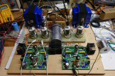
Interestingly, the original schematic (also attached) showed 82k source resistors. Assembled PCB picture too.
Thanks.
After a couple of years of working on other people's projects I've finally got around to my search for an output stage for my Universal Driver Boards.
WRT the MOSFET source resistors, R30 and R38, the original BOM, which I've attached for ease of access, stated:
"Sets the idle current through the MOSFET. You want 10mA to 20mA at idle, less if there is a secondary current path like a screen grid"
Given a secondary current path, like a screen grid, how do I work out the value of the resistors?
I'm currently running ±150V MOSFET supplies with 12k resistors which gives me a current of 12.5mA with ~2W dissipation in both the MOSFETs and the source resistors.
In my simulation at least, reducing the MOSFET idle currents doesn't have much impact on the load distortion. I haven't played around with the source resistor values in my test board yet because I don't maintain a large stock of 2+W resistors.
Interestingly, the original schematic (also attached) showed 82k source resistors. Assembled PCB picture too.
Thanks.
Attachments
The Gm in a mosfet will change with the current through the fet. Some mosfets can emit a burst of high frequency oscillation at turn on or turn off if they transition through cutoff during an audio cycle. This can also occur if the load on the mosfet goes through a rapid change in impedance, such as a control grid transitioning through zero in an AB2 situation. It is desirable to keep some current flowing through the mosfet at all times, even if the tube it's driving is cutoff.
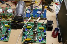
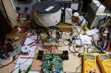
I was doing a lot of high power screen drive experiments with this board and it's predecessors. Here the screen voltage is driven highly positive (+250 to 300 volts) during peak current on the driven half cycle. It will swing almost as far negative when the other output tube is at full conduction. To avoid the condition of mosfets switching on and off, I tied that source resistor to a negative 400 volt supply, hence the 82K resistor. Note all the unusual jumpers in the first picture. The bias was adjustable from zero to a POSITIVE volt age in the 100 volt range for screen drive.
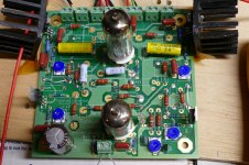
When I transitioned from screen drive experiments to conventional G1 drive the 82K resistors came out, and 12K 3 watt Panasonics went in. They were carefully chosen for the criteria of "I have a big bag full of them." Many other parts were changed for a negative bias voltage at idle.
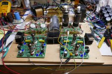
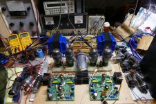
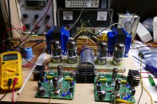
This test setup is the one that I have been using to test lots of different tubes in ordinary G1 driven AB1 and AB2 push pull. It uses a +/- 150 volt supply made with an isolation transformer. The source resistors seen in three years worth of pictures are those blue 3 watt 12K Panasonics. I have found no reason to change them despite feeding everything from tiny 50C5 radio tubes to big fat transmitting tubes. If I needed to deviate from the +/- 150 volt mosfet supply, I would change the resistor accordingly.
I was doing a lot of high power screen drive experiments with this board and it's predecessors. Here the screen voltage is driven highly positive (+250 to 300 volts) during peak current on the driven half cycle. It will swing almost as far negative when the other output tube is at full conduction. To avoid the condition of mosfets switching on and off, I tied that source resistor to a negative 400 volt supply, hence the 82K resistor. Note all the unusual jumpers in the first picture. The bias was adjustable from zero to a POSITIVE volt age in the 100 volt range for screen drive.
When I transitioned from screen drive experiments to conventional G1 drive the 82K resistors came out, and 12K 3 watt Panasonics went in. They were carefully chosen for the criteria of "I have a big bag full of them." Many other parts were changed for a negative bias voltage at idle.
This test setup is the one that I have been using to test lots of different tubes in ordinary G1 driven AB1 and AB2 push pull. It uses a +/- 150 volt supply made with an isolation transformer. The source resistors seen in three years worth of pictures are those blue 3 watt 12K Panasonics. I have found no reason to change them despite feeding everything from tiny 50C5 radio tubes to big fat transmitting tubes. If I needed to deviate from the +/- 150 volt mosfet supply, I would change the resistor accordingly.
Attachments
MOSFET source resistors
Thanks George. I understand now.
If there is a secondary current path like a screen grid the resistor needs to be smaller to get a higher MOSFET idle current.
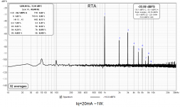
I'm doing some THD vs power measurements on a pair of 6HJ5s in crazy drive configuration with 500V HT and ±150V.
With 12k source resistors in the simulation at least the driver tubes start to clip long before the MOSFET current gets below 7mA. I can offset that by changing the operating point of the driver tubes.
I have to say that even at 1W, the simulation suggests THD for this configuration of ~7% and that's about what I'm measuring.
I'll play around with the Rg2g1 and Rg1 to see if I can improve the situation before moving on to evaluating other output stage configurations.
I'm not keen on going to 600V+ HT as others have suggested for screen drive.
Thanks George. I understand now.
If there is a secondary current path like a screen grid the resistor needs to be smaller to get a higher MOSFET idle current.
I'm doing some THD vs power measurements on a pair of 6HJ5s in crazy drive configuration with 500V HT and ±150V.
With 12k source resistors in the simulation at least the driver tubes start to clip long before the MOSFET current gets below 7mA. I can offset that by changing the operating point of the driver tubes.
I have to say that even at 1W, the simulation suggests THD for this configuration of ~7% and that's about what I'm measuring.
I'll play around with the Rg2g1 and Rg1 to see if I can improve the situation before moving on to evaluating other output stage configurations.
I'm not keen on going to 600V+ HT as others have suggested for screen drive.
Attachments
The SPP and the Universal Driver boards are both available. Unfortunately most of the original documentation for the SPP was lost in a computer incident nearly 15 years ago. So what's on the web site and here on the forums is all there is for now.
I have gathered info for the UD board and some new stuff for the SPP, but I'm having a good bit of trouble with dexterity in my hands so typing and soldering is not easy right now. I have pretty much given up on playing the guitar.
I have gathered info for the UD board and some new stuff for the SPP, but I'm having a good bit of trouble with dexterity in my hands so typing and soldering is not easy right now. I have pretty much given up on playing the guitar.
Lost ac output
Don’t know if anyone has run into this problem – it’s probably not unique to the UDB 2015 – but I thought I’d ask here. I built a couple a pair of UDB, KT-88, pentode-wired, mono block amps. I’ve had pretty good service from them for a couple of years, but always wanted to experiment with feed back. Prior to moving ahead, I wanted to establish some baseline distortion/power measurements. I ran both amps at full power into individual, 200w/8 ohm dummy loads for several tests. At some point, for Amp 2, the scope showed a sudden drop of about 50% ac output power. In that amp, I found that one of the 100r/10w plate resistors on my rectifier tube had been in contact with the B+ lead to the OPT (Hammond 1650RA) and the plate and screen leads of one of the two power tubes. All three leads were badly scorched. I removed and repaired all the burned sections, turned it back on and all was well – correct ac output. However, next day I was back to 50% power and haven’t been able to fix it since. As it stands now, for both amps, all ac and dc voltage readings on the driver boards and power tube grids are the same. However, on the problem amp, the ac readings at the plate and screen (for both power tubes) are a little less than half of what they are on the good amp. Googling around, I read that it might be a coupling cap; so I checked both of those as well as Q1 & Q2, but all those parts test OK.
Don’t know if anyone has run into this problem – it’s probably not unique to the UDB 2015 – but I thought I’d ask here. I built a couple a pair of UDB, KT-88, pentode-wired, mono block amps. I’ve had pretty good service from them for a couple of years, but always wanted to experiment with feed back. Prior to moving ahead, I wanted to establish some baseline distortion/power measurements. I ran both amps at full power into individual, 200w/8 ohm dummy loads for several tests. At some point, for Amp 2, the scope showed a sudden drop of about 50% ac output power. In that amp, I found that one of the 100r/10w plate resistors on my rectifier tube had been in contact with the B+ lead to the OPT (Hammond 1650RA) and the plate and screen leads of one of the two power tubes. All three leads were badly scorched. I removed and repaired all the burned sections, turned it back on and all was well – correct ac output. However, next day I was back to 50% power and haven’t been able to fix it since. As it stands now, for both amps, all ac and dc voltage readings on the driver boards and power tube grids are the same. However, on the problem amp, the ac readings at the plate and screen (for both power tubes) are a little less than half of what they are on the good amp. Googling around, I read that it might be a coupling cap; so I checked both of those as well as Q1 & Q2, but all those parts test OK.
Last edited:
- Home
- More Vendors...
- Tubelab
- Tubelab Universal Driver Board, 2015 version