Good work, it looks like the trick for effective AGC with dual gate mosfets is indeed that Vg2 can be lower than Vg1 due to V(AGC). With source connected to ground, 0.5 V on g1 is enough, and keeping Vg2(max) at a value so that maximum dissipation isn't exceeded. I simulated the issue, with the BF992 at Vg1=0.5 and Vg2=2.5 Id=22 mA IOW in that case no more than 10V for Vd allowed. The difference in behavior is remarkable as well when simulating an AM signal. About 450mVp is the maximum of the signal on g1 before distortion starts to become visible.
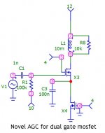
This novel "never published anywhere" AGC for mosfet will solve all issues. Instead of a pinch-off control like used with variable u pentodes, this circuit aims to keep the current through the mosfet at the same value due to insertion of a (constant) current source at the source. With control voltage at node 3 between 0 and 2V (0V works as "delay" voltage) X3 has maximum gain, in this circuit ~43 dB. By increasing the control voltage, gain goes down. 10V control voltage remains below the gate-source breakdown voltage but in this circuit, gain then is ~-18 dB. IOW over 60 dB AGC range, and those who still want more, can get an extra ~20 dB by downregulating Vg2 of X4.
Attachments
So, the current source MOSFET can be a low voltage type, maybe a BF2040 5 volt part?
Looking like a crucial witness is sick and probably can't attend court, so I may get some time to play with this sooner than expected.
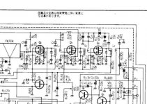
Just to throw another log on the fire - attached is the schematic of the IF strip of the Mizuho SG-9 main board. It's AGC is applying an increasing negative voltage to gate 1 of the dual gate mosfet, and gate 2 has a constant fixed voltage. The FET's are 3SK49 which looks to be a garden variety 200 MHz, 20 Vds, 40673 type part. The diode depicted looks to cross reference to an 8 volt zener, which seems a reasonable choice in that position.
This AGC is super simple and works quite well - a little fast for my taste, but not enough for me to go in and fiddle with the time constant.
I had to fix it earlier in the project ( the SG-9 came from a scrapper radio ), but I didn't pay any real attention to it other than fixing it.
Looking like a crucial witness is sick and probably can't attend court, so I may get some time to play with this sooner than expected.
Just to throw another log on the fire - attached is the schematic of the IF strip of the Mizuho SG-9 main board. It's AGC is applying an increasing negative voltage to gate 1 of the dual gate mosfet, and gate 2 has a constant fixed voltage. The FET's are 3SK49 which looks to be a garden variety 200 MHz, 20 Vds, 40673 type part. The diode depicted looks to cross reference to an 8 volt zener, which seems a reasonable choice in that position.
This AGC is super simple and works quite well - a little fast for my taste, but not enough for me to go in and fiddle with the time constant.
I had to fix it earlier in the project ( the SG-9 came from a scrapper radio ), but I didn't pay any real attention to it other than fixing it.
Attachments
The current source can even be made with BJT + diode or 2 X BJT. It isn't critical because the of the decoupled source. Very long ago I was living close to a MW transmitter, 300mV on the "wire in a tree" antenna. The 1st IF had to face an input voltage no existing stage could handle - experiments led to the above. You're right about the speed: the control curve (Vcontrol vs Gain) is far from linear. The fast change happens in the region where Vg2 becomes lower than Vg1. For a first stage you can set up a proper control network with delay in a way that even with 1V rms input, no overload occurs. Hence the region 0...2V with little change in gain is useful because AGC in a first stage shouldn't influence the S/N of the demodulated signal.
That's the way I do it in my new 432 MHz transverter.
It is based on a HP/Agilent app note. Some PIN diodes do not work
at a MHz or below because of carrier lifetime.
Current starved MOSFETs are not the way to linearity.
My new transverter board was sent to JLCPCB yesterday afternoon,
this afternoon they were already applying the solder mask.
2 different designs, 10 boards each, €20 all included. WOW.
Gerhard
Attachments
I needed a method of adjusting the gain of a linear RF power amp in a 100 watt (peak) LTE transmitter at 760 MHz. I used a voltage variable RF attenuator chip from RFMD (now Qorvo). Data sheet is too big to include here. I stuck one of these between two 50 ohm gain blocks in the path.
RFSA2013 - Qorvo
RFSA2013 - Qorvo
... Current starved MOSFETs are not the way to linearity. ...
... I used a voltage variable RF attenuator chip from RFMD (now Qorvo) ...
If the device is just being used ( mostly ) as an attenuator, is linearity that important? Since it is part of a feedback loop, won't the loop force it to be linear?
I have some Mini Circuits MAR-1+ MMIC's in my Mouser shopping cart, but it does not look like Mouser carries the part used in Gerhard's attenuator, and the Quorvo part George listed I have no chance of using on these breadboards.
Does anyone know of a suitable replacement that could work on these breadboards? I do think I have a good quantity of discrete PIN diodes ( somewhere ), but they would be old parts - late 80's early 90's vintage in the TO-92 case with only two legs.
Most PIN diodes can be used as attenuators but some, especially those designed to be used as switches may have a very narrow range of attenuation. The only way to find out is to try them.
Mini-Circuits still has some canned voltage-variable SMD attenuators that are big enough to be breadboard friendly.
LTE, CDMA, and many other advanced modulation systems run AM and FM (PM) at the same time. Often multiple RF carriers are summed together and stuffed through the same RF power amp. It better be very linear or all the signals will be blended together creating "out of band emission." The OOBE specs for cellular transmitters is pretty tough, and specced in absolute power levels, so that more RF power requires a cleaner transmitter.
I was working on a full duplex radio with a few added constraints. It all went into the trunk of a cop car. The radio needed to be capable of transmitting LTE at 765 MHz, transmitting FM at 740 MHz or 815 MHz, receiving FM at 790 or 860 MHz, and receiving LTE at 720 MHz, ALL SIMULTANEOUSLY through a COMMON ANTENNA! I had two prototypes working on my bench when the project got stuck in legal hurdles due to a large US cell phone company's threat. I left Motorola before that was settled.
The LTE transmitter I was working on at the time ran open loop at nearly class A bias. Feedback becomes a bit more tricky when the bandwidth of the transmitted signal gets large. Pure RF feedback was rarely used, at least back 10 to 12 years ago. We did build some "cartesian feedback" transmitters. The forward path is a conventional I/Q modulator accepting two baseband signals from the DSP's D/A convertors and making RF. The transmitter's output is sampled at the antenna port with a coupler. That RF is then demodulated fed to a A/D converter, and then back into the DSP. The "feedback" is done in digital magic and slick software. It worked great on the 200 KHz wide iDEN channels of the day. Our LTE was a 5 MHz channel, and the mobile DSP couldn't handle the task at an acceptable current and heat level.
Today's LTE channels have grown to 20+ MHz wide, with 50 and 100 MHz channels on the horizons for mid band 5G LTE. This is too much for even today's DSP tech to handle without melting. Even 20 years ago the cellular carriers started getting cognizant of power costs. I know that Nextel's power bill for the state of Florida alone was over a million dollars a month. It's cheaper to build a 120 watt transmitter and run it at the 40 watt level. My 100 watt peak, 10 watt average, 4 watts to the antenna (two lossy duplexers) transmitter used 180 watts worth of silicon.
If the device is just being used ( mostly ) as an attenuator, is linearity that important? Since it is part of a feedback loop, won't the loop force it to be linear?....
There's a signal path, and a control path.
The control path is amenable to NFB. (Not always easy, but possible.)
The signal path is hard to apply NFB on, because NFB depends on gain, and the gain is changing. (Or attenuation, which is the same minus some constant.)
The only way to find out is to try them.
It's taken me this long just to FIND them.
They may or may not even be PIN diodes. The bin I located them in had 21 TO-92 case Batwing MBD101, a half dozen leaded HP 5082-2835, and 9 two leg TO-92 devices that are unmarked except for some paint stripes. I distinctly recall buying PIN diodes three or four decades ago, so I am guessing the unmarked diodes are the PIN types.
edit: it is also possible they could be unmarked varactor diodes. I'm thinking not likely since these were in a bin with the Schottky's, but is there a way to differentiate between the two?
When I get a chance, I'll reconfigure that test IF board to try them out.
I printed up a preliminary breadboard so that I can have something to mount the boards on and begin to test them for function.
I scored a dozen genuine Central Semi 2N3866 transistors on eBay, so in addition to the may or may not be 2N3553 parts from AliExpress, I now have some transistors to burn experimenting with a push pull PA for the transceiver.
Attachments
Last edited:
a half dozen leaded HP 5082-2835
I remember that number from my past. Those were the magic diodes needed for getting free HBO in say 1980, back when they weren't even a 24 hour channel.
The details of building a Multipoint Distribution System receiver for the two NTSC video channels at 2.15, and 2.156 GHz with plans for a simple receiver were in one of the ham radio magazines back in 1978 or 1979. I can't find it now with a simple internet search, but it wouldn't matter today, those frequencies are used for cell phones now.
Have you guys looked at the asking prices for these old schottky diodes?
I thought $50 bucks for a steel case TO-3 regulator was off the deep end insane, but take a look at the asking prices for these diodes ... We are all sitting on fortunes in our junk boxes.
I'm pretty sure I got the 5082-2835 and mbd 101's to attempt to make homemade DBM's.
I thought $50 bucks for a steel case TO-3 regulator was off the deep end insane, but take a look at the asking prices for these diodes ... We are all sitting on fortunes in our junk boxes.
I'm pretty sure I got the 5082-2835 and mbd 101's to attempt to make homemade DBM's.
Yes, I was not condoning illegal operation but answering the point made that RF transmitters are not really DIY items. They are, but only for those who know what they are doing - which includes staying within the law. For almost everyone that means either fairly low power (almost zero power in the UK) or legitimate amateur radio. It is unlikely that a DIY transmitter for the FM broadcast band with significant power would be legal in almost any country.
The problem with DIYAUDIO RF is it can affect other RF stations if its too strong or the wrong frequency.
Audio amplifiers (unless oscillating) dont affect other amps.
I built up a hybrid amp with valve and tda7294.
I had reduced the gain of the tda7294 to adjust for gain in valve.
The thing oscillated like mad.
The oscillation from tda RFed back into valve and caused havoc.
The tda has a minimum gain and I was below that gain and so it oscillated.
I put 1nf across tda + - inputs and that fixed it.
I had reduced the gain of the tda7294 to adjust for gain in valve.
The thing oscillated like mad.
The oscillation from tda RFed back into valve and caused havoc.
The tda has a minimum gain and I was below that gain and so it oscillated.
I put 1nf across tda + - inputs and that fixed it.
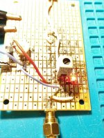
So it works a lot better now. I think this is a BF998 transistor; I've burned up a few and the marks are no longer readable on this one. But I think it is a BF998.
The best technique is to put the source at DC ground through the LED, and then bypass it for RF. The value of the resistor connecting the source to gate 1 becomes mostly unimportant, and can be set to the impedance of the preceding stage for easy impedance matching. Right now I am using 2000 ohms. That value would have resulted in no gain in the prior iteration.
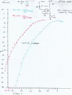
I tested with blue and red LED's, and regraphed everything. It does appear very practical to time the AGC according to the color of the source LED. Red shifts the gain curve to the left. I did not test LED colors between blue and red. Presumably the curve could be shifted right by using 1N4148 or similar diodes, but I did not try this.
Presently, a cheapo 0805 AliExpress red LED yields 26 dB gain, and 46 dB attenuation. A cheapo 0805 blue LED gives 24 dB gain, and 48 dB attenuation, the spread in each instance being 72 dB. This seems pretty remarkable for such a simple circuit with just one forty cent transistor.
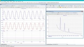
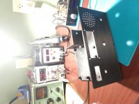
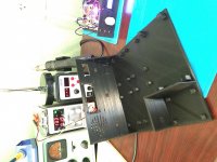
I'm using a slug tuned IF transformer to tune out the funky harmonic distortion that comes and goes as the AGC varies, and it seems to have accomplished that purpose. The circuit looks very satisfactory on both the scope and spectrum analyzer. The picture is bad but there is really not much to see.
I'm undecided whether or not to complete building out a simple IF strip with these MOSFETS, or to make another IF strip similar to the MMBT5179 first IF amplifier, and using PIN diodes as attenuators.
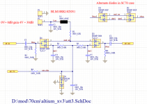
I don't know that I could squeeze a PIN diode attenuator into the XVTR board between the mixer and BF992 pre driver, but it might be feasible to use this technique to add ALC to the transmitter without much rework.
I'm still not able to make the "normal" dual gate MOSFET AGC circuit work for these devices. I've tried pretty hard with no success.
The best technique is to put the source at DC ground through the LED, and then bypass it for RF. The value of the resistor connecting the source to gate 1 becomes mostly unimportant, and can be set to the impedance of the preceding stage for easy impedance matching. Right now I am using 2000 ohms. That value would have resulted in no gain in the prior iteration.
I tested with blue and red LED's, and regraphed everything. It does appear very practical to time the AGC according to the color of the source LED. Red shifts the gain curve to the left. I did not test LED colors between blue and red. Presumably the curve could be shifted right by using 1N4148 or similar diodes, but I did not try this.
Presently, a cheapo 0805 AliExpress red LED yields 26 dB gain, and 46 dB attenuation. A cheapo 0805 blue LED gives 24 dB gain, and 48 dB attenuation, the spread in each instance being 72 dB. This seems pretty remarkable for such a simple circuit with just one forty cent transistor.
I'm using a slug tuned IF transformer to tune out the funky harmonic distortion that comes and goes as the AGC varies, and it seems to have accomplished that purpose. The circuit looks very satisfactory on both the scope and spectrum analyzer. The picture is bad but there is really not much to see.
I'm undecided whether or not to complete building out a simple IF strip with these MOSFETS, or to make another IF strip similar to the MMBT5179 first IF amplifier, and using PIN diodes as attenuators.
I don't know that I could squeeze a PIN diode attenuator into the XVTR board between the mixer and BF992 pre driver, but it might be feasible to use this technique to add ALC to the transmitter without much rework.
I'm still not able to make the "normal" dual gate MOSFET AGC circuit work for these devices. I've tried pretty hard with no success.
Attachments
... Some PIN diodes do not work at a MHz or below because of carrier lifetime. ...
All the new PIN diode parts ( at reasonable prices ) that I am looking at are only specified down to about 1 MHz, some are only good down to 10 MHz or so. The below 1 MHz parts are out of my price range for a hobby project.
I'm thinking a reasonable way forward is to make the 455 KHz IF board out of these MOSFET's with this type of LED / AGC control, and ( attempt ) to make a more modern type of board for 9 / 10.7 MHz with the MMBT5179's or similar, and the diodes I already have for the gain control. If the ones I have on hand don't work, then I'll buy some modern ones.
It looks like the AGC voltages are more or less compatible for both types of parts.
- Home
- Member Areas
- The Lounge
- No RF gear here?