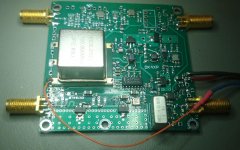
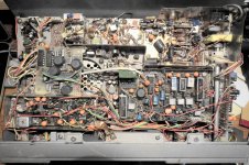
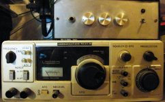
I just got first FR4 from JLCpcb for my RedPitaya 432 MHz transverter. First version was
home-etched. Completely no-tune. Oscillator is a 100 MHz crystal oven with CMOS
output. Buffered with some paralleled inverters, two doubler stages with balun and two
diodes, SAW-filter to clean the osc on 400 MHz.
For RX and TX each an TUF-1H mixer and an SKY MMIC as LO buffer.
RX is 2*SKY67150, 2 SAW-Filters, pin diode attenuator, low pass and maybe an
optional 20 dB gain stage if the RP is too deaf. THe 2 RX filters deature an
impressive selectivity.
TX has 1 SAW Filter after the mixer and then 2 MMICs. TX power probably 0.5W.
There is an alterative MMC from Hittite/AD that delivers 1.6W in SOT-89 also from 5V,
but not so easy and hotter.
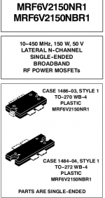
My 150W TX power transistor was declared obsolete by NXP a week after I bought it.

The board runs from 5V, the oven currently from 3V3 since I had it. There is a 5V
version, too.
The RX noise figure is 0.6 dB. The SKY eval board features 0.3 dB. I can't get better,
no matter what I do. I even swapped parts with the eval board.
home-etched. Completely no-tune. Oscillator is a 100 MHz crystal oven with CMOS
output. Buffered with some paralleled inverters, two doubler stages with balun and two
diodes, SAW-filter to clean the osc on 400 MHz.
For RX and TX each an TUF-1H mixer and an SKY MMIC as LO buffer.
RX is 2*SKY67150, 2 SAW-Filters, pin diode attenuator, low pass and maybe an
optional 20 dB gain stage if the RP is too deaf. THe 2 RX filters deature an
impressive selectivity.
TX has 1 SAW Filter after the mixer and then 2 MMICs. TX power probably 0.5W.
There is an alterative MMC from Hittite/AD that delivers 1.6W in SOT-89 also from 5V,
but not so easy and hotter.
My 150W TX power transistor was declared obsolete by NXP a week after I bought it.
The board runs from 5V, the oven currently from 3V3 since I had it. There is a 5V
version, too.
The RX noise figure is 0.6 dB. The SKY eval board features 0.3 dB. I can't get better,
no matter what I do. I even swapped parts with the eval board.
Attachments
Last edited:
Some questions ...
+17 dBm mixers ... is there a relationship between LO power and strong signal capability of the mixer? In other words, does more LO power mean the mixer can take more power on the RF port ?
On the TX strip ... what is the purpose of all the vias on the ground / heat sink? Is this to tie the layers of the board together so they do not become a capacitor or capacitors?
That relationship exists, because the current through the mixer diodes is the (vector) sum of RF input and LO signals. What also matters is not to exceed the maximum LO power. Probably even more important is that all ports of the DBM are terminated with 50 ohm. When not, reflection occurs, deteriorating performance. To keep things simple, I always terminated the IF of a diode DBM with a grounded gate jfet amplifier (20 mA/V transconductance). Back then, the P8000 was a favorite - would still be when available.
That P8000 termination probably came from the commercial/military shortwave
receiver development at AEG/Telefunken and/or Rohde&Schwarz in the early 70s.
Methinks Prof. Ulrich Rohde was involved into this. He is still active and a worthy
goal for google searches. In ham radio that was promoted very prominently by DJ7VY,
such as this:
< https://www.google.de/url?sa=t&rct=...06_DJ7VY.pdf&usg=AOvVaw2CTQ-jLfxPKrmHFQ0WVald >
Sorry, it's in German. I can help translating if there are questions.
I still have some P8002. Never used most of them. Texas Instruments denies
parenthood. It's a pretty lame transistor by today's standards. But gm=20mA/V
at 50 mA happens to fit nicely as a common gate 50 Ohm termination.
Teledyne CP643 was similar.
The TUF-1H has abs.max. = 23 dBm, that is 200 mW oscillator power, but normally
only 50 mW. More osc power means more intercept point, everything else equal.
MCL has mixers upto 27 dBm nominally ( VAY-1 IIRC). That's half a Watt.
Everybody will hear you listening.
But with less than the nominal power, a smaller mixer may fare better.
The LO port does not need precision termination and no sine signal. It does
it's best to prohibit a sine by being mostly a short when the diodes start
nicely conducting.
On 432, all generated frequencies are far from each other, so it is easy
to terminate them in a passive way. The bandwidth of the mixer is only
some 800 MHz, so the phase relationships won't be too precise.
Many of the vias are there for thermal reasons, the many SOT-89 produce some heat.
I had planned a Hittite chip for the PA that could deliver 1.6W, but that went probably
too far.
cheers,
Gerhard DK4XP
Last edited:
Correct, at the time of those developments on mixers and low phase noise oscillators I was working as designer for Elektuur magazine (now Elektor) so read the publications. The job enabled me to order about anything so I got TI P8000, U350, E430 and diode mixers - even have an "unobtanium" like the XRS2000.
Ulrich Rhode also wrote an article comparing Ed Oxner's jfet mixers with diode mixers. I measured a lot with the spectrum analyzer and even included the venerable 7360 beam deflection tube in the comparisons. I soon discovered that when patient enough to match a quad of BF247C jfets, it was possible to construct a very high level DBM with lower noise than from a combination of diode mixers and grounded gate fets.
Dead bug mounting as the mixer would require up to 1 W from the power supply. Next came the development of very low noise dual gate mosfets (BF9 series). They too could be used for high performance mixers and without the issue of port reflection. So I still have several P8000, U350, BF246C, SRA3, VAY1, SBL1 with little use for them.
What was amazing, Ulrich Rhode also wrote an article about noise blanker improvement: instead of a fast "on/off" switch somewhere in the IF chain, implementation of that switch in the LO chain. Obvious advantage, no leakage of the control pulse in the signal. I haven't seen that applied in any receiver.
Last edited:
Gilbert cell mixers are very clean indeed and also can be very low noise when fitted with the proper (matched) jfets. With (matched) dual gate mosfets a DBM is even simpler as you don't need the "bottom" section. Already in the 1970s Siemens had the bipolar SO42P (look it up) as a mixer up to VHF. I Used it extensively also as phase detector.
Gilbert cell mixers go back to 1963 and this patent. Gilbert made notable improvements on this patent several years later.
https://pdfpiw.uspto.gov/.piw?docid=03241078&PageNum=1
They were popular well into the 2000's with the NE/SE602 being the most popular. The MC1496 was also very common.
I spent 41 years at Motorola most of that as a design engineer. The Gilbert cell became the limiting factor in two way radio design in the late 2000's as high intercept point LNA's got cost and current drain competitive. We went back to the diode DBM for a couple designs, then switched to a 4 fet DBM, which is now buried deep inside an RF IC. The drive, and timing thereof is a trade secret and product of two or three years of research.
A police walkie talkie needs to receive a base station that could be 20 miles away, but the cop may be standing in the middle of a jungle of cell towers and TV transmitters that may be 5 MHz or less away. IMD (the same stuff that muddies up our sound) will blend all those powerful transmitters together making RF mud that covers up the weak base station.
Ham radio equivalent.....big pileup on contest day when you are trying to hear a weak signal on the other side or the planet just a few KHz (ssb) or Hz (CW) away.
Those were the times - in Europe where I was living, field strengths were extreme so communication receivers required very linear mixers. The little known TCA240 still is a good choice when using the "bottom" section for signal and the "upper" section for LO. Ulrich Rhode published a DBM with 4 BJTs, with (resistor) feedback over every BJT. There's also the DBM with lossless feedback by Chris Trask - RF transformer nirvana. Not exactly "integrated on chip" friendly but re performance can be excellent...
What also became apparent was the requirement of clean transmitters (noise sidebands). Here (in Panama) that's a major issue although not the number 1 (that's powerline interference, and none of my receivers can eliminate it).
What also became apparent was the requirement of clean transmitters (noise sidebands). Here (in Panama) that's a major issue although not the number 1 (that's powerline interference, and none of my receivers can eliminate it).
... Completely no-tune ...
Snow / ice bound this week, so I have been working on untuned IF amplifiers the last couple of days, with not much to show for it.
I started with an MC1350, and was able to get about 30 dB gain out of it, but overall, I wasn't very happy with it, so I abandoned it for now.
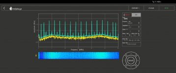
I have a BF998 untuned amp working reasonably well - but not at the frequencies I want it to work at. I want the the filters to determine the frequency of operation - 9 MHz and 10.7 MHz for sure, and 455 KHz would be nice if that big a spread could be accommodated.
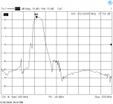
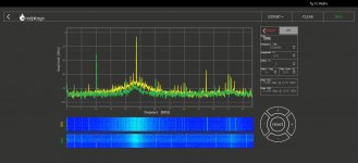
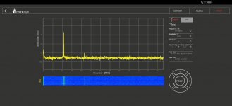
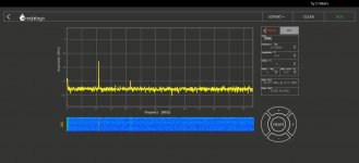
The pics show the 10 MHz output of the RP looped back into the number 2 input as the green trace, and then frozen as the reference point, at about - 31 dBm. The yellow trace shows the same signal at the output of the untuned amp. At 10.7 MHz, it only has 8 or 9 dB gain, but at 23.5 MHz it has about 25 dB gain, which looks reasonable. This is a fairly broad peak, about 5 MHz wide.
So how do I move the peak down? The load is about 15 turns on an FT-23 toroid, with a three turn link for the output. Should I tighten the coupling by adding some more turns on the link, or use more inductance? I would probably have to move up to an FT-37 toroid, I don't think more turns on the FT-23 will add much inductance.
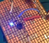
The circuit is a little showy, the source and gate 1 are both floated a couple of volts above ground by the blue LED, and are bypassed for ac with 100 nF caps. I don't think any of that would affect the frequency response. The voltages all look right: 3.15 vdc on the source, 2.25 vdc on gate 1. Gate 2 is biased to one half the B+ (12 vdc) which should produce maximum gain. Current seems low - it's only pulling 4.5 ma. Most of the parts are 0603 to get some experience with smaller parts. I think 0603 is as small as I want to go without some sort of visual aid.
Attachments
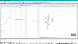
Win, could you provide more info to get the amplifier right? Dual gate mosfets are high impedance devices so for optimum performance this must be taken into account. Will the amp be used with AGC? What are input and output impedance? To illustrate the issue, this simulation.
Attachments
Yes - this stage(s) will be AGC controlled, right now I am using a divider to provide a fixed "AGC" voltage of one half the B+ voltage to gate 2.
This stage will be fed from a crystal filter ( or mechanical filter ), but I'm not sure what filter or what frequency at this point - I expect it will be 250 to 1000 ohms. I have a 1000 ohm resistor from gate 1 to ground for now.
I got rid of the funky LED bias, to eliminate that as a variable, but may play some more with it later. The source is ac bypassed with 100 nF. The FET is an Infineon BF998 bought from Mouser, so I assume its genuine.
I rewound the transformer load - its now 14 turns primary and secondary on an FT37-23 core, so 1:1 ratio. ( just for fun, I tried it as a 4:1 bifilar transformer, and got a funky double hump at 4 and 23 MHz. I didn't pursue that, as it seemed like the feedback would just fight the AGC when I get around to that.)
Results are a little better now, and relative to your sim, are a little better in terms of gain, but worse in frequency response. I'm only getting about 4 to 25 MHz at good gain. The input is - 31 dBm, so I'm seeing about 19 dB gain across the bandwidth of the amp. I can eke out another 1 dB of gain by increasing the current in the FET to 7 ma - these RP screen shots were taken at 4.5 ma.
I'm going to play some more with it tonight or tomorrow. I was hoping to get enough gain to need only 2 IF stages, but it looks like I'm going to need 3.
Attachments
For a high AGC range, the standard circuit is with the source at a positive voltage, LED is OK. Gate 2 then can be below source voltage for maximum AGC range. Because of the high output impedance, the value of the coupling capacitor from the drain coil is important. Too low and a resonance at the load resistor shows up, too high extends the bandwidth to the lower frequency region but at the cost of less gain at for instance the 455k IF. At the high end, Cds and the drain coil can form a resonance. Many crystal filters have slightly inductive in-and output so require trim caps. With a two-stage tuned BF998 IF it's not difficult to get 80 dB of IF gain but that's still too low and the AGC might pose stability problems.
I was using a 100 nF cap at the output, so I removed that and replaced it with a 33 pF cap. This made some subtle difference - the gain response was a little smoother across the usable bandwidth, but it didn't do much to extend the frequency response. I was also using a 100 nF on the input, and I changed that to 100 pF, but it didn't make any difference that I could tell.
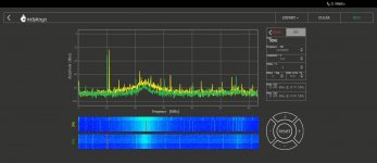
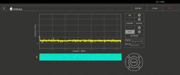
I changed the decoupling a little bit, and I replaced the BF998 with a BF992, but other than reducing the noise floor some, I can't tell that I've made much difference. The RP screenshots show the -31 dBm generator output looped back into input 2 and frozen, and then the output is applied to the amp and the amp output is applied to input 1 for comparison. These were taken with a BF992 in place. I look to be stuck at about 19 dB gain at HF, but at 455 Khz it has negative gain.
My filters fall into three groups - a bunch of crystal filters between 9 and 10.7 MHz. A bunch of Drake filters that are between 5 and 6 MHz, IIRC. And then the Collins mechanical filters that are between 250 and 500KHz.
I'm thinking it might be more realistic to make two IF boards - one for the HF filters, and one for the LF filters. I have some BF2040 and BF1105R FET's with me to try out. In the meantime I may also play with some of those multifunction IF / AM Detector IC's.
Attachments
Filters need a proper termination - if not, flatness suffers a great deal. It's very audible and (in my case) extremely annoying. So much of my design effort goes into proper termination of filters. Using tuned IF coils simplifies impedance transformation and the tuning procedure guarantees maximum flatness. That means separate IF amplifiers. For a 2nd IF <2MHz the TCA440 (Siemens) is ideal. It's fully symmetrical, implying very effective and fast (attack) AGC without motorboating (great for SSB and CW). It handles 50 MHz at the input and is easy to use with for instance ceramic filters. As the 2nd IF is broadband (to 2 MHz), detectors have to be fitted with an LPF to remove "out of band" noise. Long ago I modified an R1000 along this line (still works but sold to a friend before emigration).
Attachments
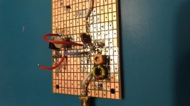
I moved the goal post from no tune, to some tuning, and put an adjustable tuned circuit at the input to make it easier to go from the output of a low impedance filter to the MOSFET. The toroid is a T30-6, the ratio between the windings is 1:5, and the trimmer cap is sitting on top of a fixed cap, giving enough range to tune to both 9 and 10.7 MHz. A 1K resistor between the secondary and ground is a placeholder to substitute for a filter load.
The usual dual gate mosfet amplifier circuits in the amateur literature depict the devices either with no bias on gate 1, or just a high value resistor from gate 1 to ground, and then a variable positive AGC voltage on gate 2. My BF992, when wired in this manner, would not show any gain variation when a simulated AGC voltage was applied to gate 2. As long as there were a few volts positive on gate 2, the BF992 would run at maximum gain. At first I thought I had a bad BF992, but I tried several and they all responded the same way. I did not run into this anomaly when I built out the transverter for the SG-9 IF board, because the RF amp there does not use AGC - it runs at max gain all the time.
The only way I could get the BF992 to respond properly to an AGC voltage applied to gate 2, was to apply a small positive voltage on gate 1. When that is done, it works as expected. A voltage divider works well here, but it is more convenient to float the source above ground with an LED, and just take the positive voltage from the top of the LED through a resistor to gate 1. The value of this resistor makes some material difference, generally speaking the higher the value the better. So I don't know if all the published literature is wrong, I'm doing something wrong, I have some funky BF992, or these last generation MOSFETS are subtly different from the earlier ones.
Anyway, when set up to work, it looks like one BF992 is good for about 45 to 55 dB range of gain / reduction. The AGC voltage on gate 2 needs to range from at least 1 to 4 volts. The resistor from the top of the LED to gate 1 alters the relationship between gain and reduction. I settled on 100K which gives 17 dB gain, and 33 dB gain reduction. A 22K resistor gave 14 dB gain, and 40 dB reduction. It may be possible to use this characteristic to delay the AGC across multiple transistors, and different color LED's might also be useful.
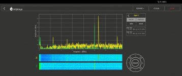
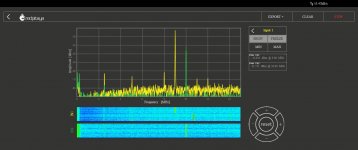
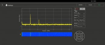
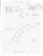
One other interesting characteristic - at maximum gain the BF992 has no harmonic distortion, but there is a region where reverse AGC is applied that does not cause gain reduction, but instead produces a second harmonic, which increases in amplitude with increasing reverse AGC, until gain reduction begins at which point the second harmonic reduces faster than the fundamental. This behavior occurs whether or not the source is floated above ground with an LED or not, and whether or not gate 1 is biased from a divider or from the LED. If the latter, it does appear that higher values of the bias resistor may increase this effect. This behavior seems undesirable in a broadband IF strip.
I put some screen shots up showing this oddball behavior, and attached a page from my notebook showing a gain plot with the LED bias and a 22K resistor.
The usual dual gate mosfet amplifier circuits in the amateur literature depict the devices either with no bias on gate 1, or just a high value resistor from gate 1 to ground, and then a variable positive AGC voltage on gate 2. My BF992, when wired in this manner, would not show any gain variation when a simulated AGC voltage was applied to gate 2. As long as there were a few volts positive on gate 2, the BF992 would run at maximum gain. At first I thought I had a bad BF992, but I tried several and they all responded the same way. I did not run into this anomaly when I built out the transverter for the SG-9 IF board, because the RF amp there does not use AGC - it runs at max gain all the time.
The only way I could get the BF992 to respond properly to an AGC voltage applied to gate 2, was to apply a small positive voltage on gate 1. When that is done, it works as expected. A voltage divider works well here, but it is more convenient to float the source above ground with an LED, and just take the positive voltage from the top of the LED through a resistor to gate 1. The value of this resistor makes some material difference, generally speaking the higher the value the better. So I don't know if all the published literature is wrong, I'm doing something wrong, I have some funky BF992, or these last generation MOSFETS are subtly different from the earlier ones.
Anyway, when set up to work, it looks like one BF992 is good for about 45 to 55 dB range of gain / reduction. The AGC voltage on gate 2 needs to range from at least 1 to 4 volts. The resistor from the top of the LED to gate 1 alters the relationship between gain and reduction. I settled on 100K which gives 17 dB gain, and 33 dB gain reduction. A 22K resistor gave 14 dB gain, and 40 dB reduction. It may be possible to use this characteristic to delay the AGC across multiple transistors, and different color LED's might also be useful.
One other interesting characteristic - at maximum gain the BF992 has no harmonic distortion, but there is a region where reverse AGC is applied that does not cause gain reduction, but instead produces a second harmonic, which increases in amplitude with increasing reverse AGC, until gain reduction begins at which point the second harmonic reduces faster than the fundamental. This behavior occurs whether or not the source is floated above ground with an LED or not, and whether or not gate 1 is biased from a divider or from the LED. If the latter, it does appear that higher values of the bias resistor may increase this effect. This behavior seems undesirable in a broadband IF strip.
I put some screen shots up showing this oddball behavior, and attached a page from my notebook showing a gain plot with the LED bias and a 22K resistor.
Attachments
Hi,
remember not to blast the gate protection Zener diodes when trying to
check the possible AGC range.
It is known when you try to reduce the gain of a dual gate MOSFET,
IP3 first gets much worse and only later improves again.
You might find the 3 part article from U. Rohde interesting:
< Key components of modern receiver design 1 >
<Key components of modern receiver design 2 >
< Key components of modern receiver design 3 >
IIRC there is a lot more on this site.
cheers, Gerhard
Thank you, Gerhard.
I'm pretty sure I have not damaged these FET's. The Vds on the BF992 is 20, and I haven't exposed a gate to more than 6.9 VDC. The particular BF992 that these measurements were taken on has not seen a gate voltage higher than 5, or a static drain voltage higher than 9. The power supply on the prototype board uses a 78L09 which puts 8.95 VDC on the drain, and gate 2 has an adjustable voltage divider configured to supply between 4.05 and 0.75 VDC to simulate an applied AGC voltage / manual IF gain control.
The BF992 seems to be a pretty rugged part - it is used as the RF amp and low level TX amp on the transverter board for the transceiver, and in that application they run straight from the unregulated DC applied to the transceiver - as high as 14.4 VDC.
I will read Dr. Rohde's references carefully at the earliest opportunity.
Unfortunately ...
From April 17, 2018 ...
Now, almost three years later, this thing continues to be a real irritant in my life. They've filed *two* lawsuits against me, one of which is set for trial this coming week. It's been postponed many times, and may be again, but I likely won't be able to work on the hobby thing this week.
I had not planned on going down rabbit holes with these things - I just wanted to get an IF back end up and running, quick, so I could play with the ring diode mixers in the front end, but I got sucked into this when I could not get the FET's to work as expected ...
As an aside, for anyone interested in these things, the BF1105R dual gate MOSFET that I used with the NE602 / TA7642 thing has all the biasing resistors on the chip, works really well, and is still a current part at Mouser.
I'm pretty sure I have not damaged these FET's. The Vds on the BF992 is 20, and I haven't exposed a gate to more than 6.9 VDC. The particular BF992 that these measurements were taken on has not seen a gate voltage higher than 5, or a static drain voltage higher than 9. The power supply on the prototype board uses a 78L09 which puts 8.95 VDC on the drain, and gate 2 has an adjustable voltage divider configured to supply between 4.05 and 0.75 VDC to simulate an applied AGC voltage / manual IF gain control.
The BF992 seems to be a pretty rugged part - it is used as the RF amp and low level TX amp on the transverter board for the transceiver, and in that application they run straight from the unregulated DC applied to the transceiver - as high as 14.4 VDC.
I will read Dr. Rohde's references carefully at the earliest opportunity.
Unfortunately ...
From April 17, 2018 ...
... The real irritant in my life right now is some abandoned underground storage tanks - and whose property they are actually located on: mine, or a sovereign state.
Now, almost three years later, this thing continues to be a real irritant in my life. They've filed *two* lawsuits against me, one of which is set for trial this coming week. It's been postponed many times, and may be again, but I likely won't be able to work on the hobby thing this week.
I had not planned on going down rabbit holes with these things - I just wanted to get an IF back end up and running, quick, so I could play with the ring diode mixers in the front end, but I got sucked into this when I could not get the FET's to work as expected ...
As an aside, for anyone interested in these things, the BF1105R dual gate MOSFET that I used with the NE602 / TA7642 thing has all the biasing resistors on the chip, works really well, and is still a current part at Mouser.
Last edited:
- Home
- Member Areas
- The Lounge
- No RF gear here?