Ask yourself how you would bias the Vas.
Unfortunately, I'm really still a newbie when it comes to diy. I have built a few things but they were pretty well documented. I'm starting with simpler circuits so I can start understanding the basics, (such as biasing). This description is from Bruce DePalma. Does this help explain it or am I way off?
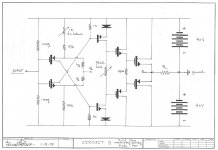
[SIZE=-1]The second stage is the voltage gain stage. Complementary bipolars should be used here to insure maximum voltage, rail to rail, drive. The second stage is interesting because it is a combination of two driven current sources using each other as load resistor.[/SIZE] [SIZE=-1]The diodes in the emitter circuit are used in a dual mode. Using complementary bipolars as recommended, these diodes provide temperature compensation in conjunction with the 1K base to ground resistors. The other function is to ensure the lowest base input resistance in the voltage amplifier stages. The current supplied to the gain stages by the input transistor pair divides between the base to ground resistor and the input resistance of the gain stage, i.e. the lower the base input resistance the more driver current flows into the gain stage transistors.[/SIZE]
[SIZE=-1]If the base input resistance were zero, all the driver current would flow into the bases and the gain of the two-stage combination would be highest. Substitution of complementary FETs in the gain stage changes the input situation since FETs are voltage actuated.[/SIZE]
[SIZE=-1]In the gain stage each transistor acts as the load resistor for the other. Very high gain and linearity is possible. Using bipolars, the drive output of this stage is almost peak to peak, rail to rail, less the saturation voltages and emitter diode voltage drops. The gain of this stage using bipolars is 1000-1500. Since the second stage operates as a current source a variable series resistor in the common collector circuit can be used to regulate the output stage quiescent current. As can be appreciated from the circuit schematic, any supply voltage variations either from mains fluctuations or long term thermal temperature co-efficient effects in the active devices appear only as a common mode effect and do not shift the d.c. balance point of the circuit.[/SIZE]
For a Vas like that to operate properly, the diode should act like a fixed resistor, sorta. Otherwise signal in, garbage out.
Common resistance is defined by Ohm's law as R = V/I.
A diode however, has two sorts of resistance ; Static and Dynamic.
The static value is the total forward voltage drop divided by the current going through it.
For a changing current value, the Vf value of a diode alters too. The dynamic resistance value is change in voltage divided by change in current (R = dV/dI)
The Vas should operate in the constant dynamic resistance range of the diode.
With a plain 1N4148, Vas bias current has to be rather high, dynamic resistance linearity of the diode sucks below ~15mA.
A Bat64 diode e.g. has a dV/dI curve that's straight as an arrow between 0.01 and ~8mA. (the Schottky also has the advantage of very low forward voltage)
The schematic is just a topology sketch. To make it work, you'd have to pick parts and redial digits.
Thank you. Do you know if anyone has built it?
Yes and it is a nice amplifier for the simplicity.
Simon7000, do you know who has built it and possible what values of transistors and diodes they used?
- Status
- This old topic is closed. If you want to reopen this topic, contact a moderator using the "Report Post" button.
- Home
- Member Areas
- The Lounge
- Mystery schematic