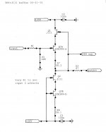
buffer schematic
Here it is.I'll get round to a schematic soon to clarify.
Attachments
cascode Q gates should connect to the respective cascoded Q's source - not the far end of the degeneration/current set R
and are you even getting 2 V Vds on the 389 with the J111? - adding some green or blue LED and few uA pullup in the J11 cascode's gates to up the V may help more
and are you even getting 2 V Vds on the 389 with the J111? - adding some green or blue LED and few uA pullup in the J11 cascode's gates to up the V may help more
Here it is.
Maybe better to cascode with depletion mode mosfets?
Attachments
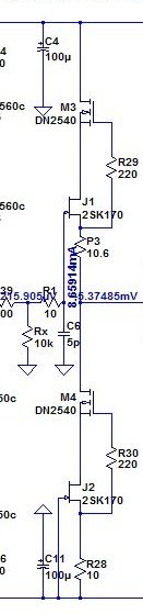
I'm seeing about 4.8V Vds on the 389V, for this particular batch of J111s. So that is well above pinchoff, although a little higher would further reduce Cdg. The quiescent current btw is about 6.6mA.cascode Q gates should connect to the respective cascoded Q's source - not the far end of the degeneration/current set R
and are you even getting 2 V Vds on the 389 with the J111? - adding some green or blue LED and few uA pullup in the J11 cascode's gates to up the V may help more
Yes, I agree the cascode gate might do better tied directly to the 389 source. I'll get to that when I have some more time, and see if there is a noticeable effect. Nonetheless, the main point of this was to see if the substrate drive helped or hindered, and for me it certainly does help. Fortunately it's easy to separate the distortion due to output loading from that due to input capacitance effects.
I'd post the Ap plots but I'm having printer problems with the XP machine running the Ap. I guess I could snap a picture.
This is not presented as a buffer amplifier design, just a breadboard to investigate the behavior of distortion as a function of driving impedance, an often-neglected area. No PCBs are anticipated
")
Brad
Last edited:
Yes, the DN parts are also an option, although I worry a bit about the body diodes. The DMOS will have a lower impedance presented to the 389 drains owing to the high transconductance, which is a benefit for the removal of Cgd effects in the 389. I'm using some Diodes Inc./Zetex enhancement mode parts in another design and biasing with a current-source-excited parallel R-C, and they seem to work well (ZVN2106, ZVP 3306).Maybe better to cascode with depletion mode mosfets?
Made that change (in fact I'd had the lower J111 gate tied to the 389 source already, it turned out---as I say I have trouble seeing this stuff).cascode Q gates should connect to the respective cascoded Q's source - not the far end of the degeneration/current set R
Essentially no change in the performance previously reported.
Yes, the 5564s have a fairly high pinchoff voltage compared to the SK389s, but indeed lower capacitance.It may be useful to try the same sort of thing with a 2N5564, and use really high Idss J111's. Less non-linear capacitance to start with. Be careful with the Idss though, the cascode must be much higher than the 2N5564.
The motivation for the larger-area parts is usually low voltage noise---but if the application is buffering a source with relatively high Z, there's likely a lot more noise in the source to begin with.
Another promising candidate: http://www.linearsystems.com/assets/media/file/datasheets/LSK489.pdf
Brad, thank you. Wow... thats a 40x improvement & counts as a material advancement in the SOTA (that I have not seen documented elsewhere.)
I will try to repeat your experiments. I dont have the J111s to hand though and fancy trying a simpler approach, so will try the 15c schematic and a cap from the output to the substrate & report. Either it was a snafu of some sort or the existance of a small DC offset at the output throwing things off for me earlier. Lets see...
Just for ref, your distortion measurements above are THD and not THD+N correct ?
An elegant solution without additional active parts so thanks again.
I will try to repeat your experiments. I dont have the J111s to hand though and fancy trying a simpler approach, so will try the 15c schematic and a cap from the output to the substrate & report. Either it was a snafu of some sort or the existance of a small DC offset at the output throwing things off for me earlier. Lets see...
Just for ref, your distortion measurements above are THD and not THD+N correct ?
An elegant solution without additional active parts
so thanks again.
Last edited:
Brad, thank you. Wow... thats a 40x improvement & counts as a material advancement in the SOTA (that I have not seen documented elsewhere.)
I will try to repeat your experiments. I dont have the J111s to hand though and fancy trying a simpler approach, so will try the 15c schematic and a cap from the output to the substrate & report. Either it was a snafu of some sort or the existance of a small DC offset at the output throwing things off for me earlier. Lets see...
Just for ref, your distortion measurements above are THD and not THD+N correct ?
An elegant solution without additional active parts
For what amounts to an open-loop buffer the performance is pretty decent, but loading will spoil it in a hurry unless load compensation techniques are used.
The distortion is indeed distortion + noise, but the amplitude is swept from 100mV to 10V rms, so the curves start coincident regardless of frequency; that is, they show the predominance of the noise, which is measured independently to be consistent. Since a 100k resistor at 300K is about 40.7nV/sq rt Hz, it overwhelms the noise of the buffer, which from the Toshiba curves and the operating current, would be expected to be about 1.1nV/sq rt Hz at 1kHz for a single device, and raised about 3dB by the noise in the lower device. So in any event it's the resistor noise that dominates the overall noise.
Once out of that you see a divergence in the THD+N for the different test frequencies, with the 10kHz a good deal higher than the 1kHz. This is consistent with the voltage-variable capacitance accounting for the nonlinearity.
Also as expected, the distortion at high levels is virtually all second harmonic. Thus in a balanced design with two such buffers this would mostly go away.
If the buffer noise needed to be lower, one could use a quieter current generator, but thereby require some alternate temperature compensation for low d.c. output drift. One notion I floated a while back in a thread about an inverting current conveyor was to use one half of a dual device to generate a current, use that to develop a filtered reference voltage, and use that larger voltage to be the voltage ref for a current generator with a lot larger series resistor than here. In this way one can get close to the intrinsic noise of a single section of the dual device, yet preserve temperature stability. But usually the contribution of a buffer like these will be small compared to other noise sources.
If you want some J111s just PM---they are cheap, easily mailed, and I have a bunch. They are from a batch with fairly high Idss, but as jcx properly expressed concern about sufficient drain-source voltage on the lower JFETs, the bracketing is so large that one could have problems with a batch that was on the low side of the spec.
Enough Semiconductors/Silicon that sounds like its ripping my head off/shaving my Cornea's etc haha.
What you need is a series resistor to increase output impedance haha. And lowering damping haha.
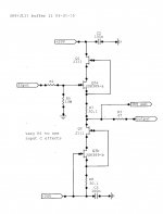
Corrected schematic with cascode gates to lower sources attached.
Brad wouldn't you call that bootstrapping rather than cascoding?
Jan
A bootstrapped cascode I guess. Walt Jung uncovered the first person to do it, as part of his work on current sources and related to the boxall-baxandall etc. stuff, Gene Csanky, who is still with us.Brad wouldn't you call that bootstrapping rather than cascoding?
Jan
Brad, ok I can confirm that it works as you suggest even with the simpler non cascode follower of 15c.
Thd @10khz with a 10KOhm drive impedance at 1vrms out was 0.014pct with substrate unconnected.
Same again but with substrate connected to output, thd was 0.002pct.
This was with the analyzer at a 80khz bw
Thd @10khz with a 10KOhm drive impedance at 1vrms out was 0.014pct with substrate unconnected.
Same again but with substrate connected to output, thd was 0.002pct.
This was with the analyzer at a 80khz bw
And at a 100k drive impedance and using the same 30khz bw you used (for comparison...)
Thd @10khz and 1vrms out = 0.39pct (heckuva lot more than your cascoded circuit)
But after bootstrapped substrate:
Thd @10khz and 1vrms out = 0.0063 thd (quite a bit of an improvement for one wire!)
My application will never see a source of more than 5-10k, and so I don't really have an urgent desire to improve things further with the cascode version.... But it's always nice to know that the option is there))
Brad thanks again....
Thd @10khz and 1vrms out = 0.39pct (heckuva lot more than your cascoded circuit)
But after bootstrapped substrate:
Thd @10khz and 1vrms out = 0.0063 thd (quite a bit of an improvement for one wire!)
My application will never see a source of more than 5-10k, and so I don't really have an urgent desire to improve things further with the cascode version.... But it's always nice to know that the option is there
))Brad thanks again....
Last edited:
Today is the perfect day to let it out and announce a stunning new amplifier topology from me, at BEAR Labs!
John, I am sure you will fully understand the implications!!
Linked for ease of locating:
http://www.diyaudio.com/forums/solid-state/272340-stunning-amplifier-development-feedforwardback-feedbackforward.html#post4279307
John, I am sure you will fully understand the implications!!
Linked for ease of locating:
http://www.diyaudio.com/forums/solid-state/272340-stunning-amplifier-development-feedforwardback-feedbackforward.html#post4279307
Bob Cordell did a fine and lengthy app note for the LSK489, by the way.linear systems needs to pay you some money to write an app note
Happy to be of help. I may write on load compensation at some point, but no more hijacking of this thread I think.And at a 100k drive impedance and using the same 30khz bw you used (for comparison...)
Thd @10khz and 1vrms out = 0.39pct (heckuva lot more than your cascoded circuit)
But after bootstrapped substrate:
Thd @10khz and 1vrms out = 0.0063 thd (quite a bit of an improvement for one wire!)
My application will never see a source of more than 5-10k, and so I don't really have an urgent desire to improve things further with the cascode version.... But it's always nice to know that the option is there
Brad thanks again....
- Status
- Not open for further replies.
- Home
- Member Areas
- The Lounge
- John Curl's Blowtorch preamplifier part II