Also, you circuit guys..I'm using a common base to turn the p fet on, with maybe a 100 ohm resistor to turn it off, and pulling the emitter with a resistor/fet combo such that the transistor never saturates. Any obvious problems or comments would be much appreciated.
I'd recommend you replace the "common base" NPNBJT (which I personally would have called a cascode device), with a "common gate" (cascode) Nchannel MOSFET. Why? Because a MOSFET costs about the same but does not fail if you accidentally violate the VEBO spec {typical value: -5 volts} during power-on or power-off.
If you switch to a MOSFET you can use a trivially simple gate bias circuit {hard-connect to +5 supply}, and you can drive the source directly from logic gates {even open collector gates!} with no current limiter/voltage limiter mechanism.
For supplies of ~40 volts or less you can use the 2N7000, and for ~150 volts or less you can use the BS107/BS108 or the ZVN0124.
Last edited:
What is the practical affect of 'skin' affect?
IMO - Mostly, it causes a pulse or impulse with fast leading edge to become time smeared. If you model each skin layer as if it were doing the same thing as an inductance... with the L decreasing towards the outer edge or surface, then you get the signal frequencies with delay changes. Or, at some layers traveling faster than other layers.
A transient pulse has the high freq travelling on the outer edge where the equivelant L is lowest. In sine wave use, such as a RF signal (carrier) you dont see much affect... but with data signals it can be a disaster to the waveform fidelity. It can lead to corruption or loss of data.
How does this become important in building audio circuitry/behavior (analog or digital audio)?
THx-RNMarsh
Last edited:
I love this thread. But it reminds me of a bunch of guys talking about women instead of just making what they have work. So what is the best audio we can design with what we have on hand? This is something you don't get from thread. I work on some pretty high level defense stuff, and we don't talk like this.
looks like one of the depictions in tom van doren's work..
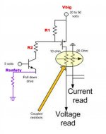
Question. I'm designing a microwire edm system, so need pulses for the spark gap which are 20 to 30 nanoseconds wide, to the tune of 20 to 50 volts. Attached is the rough scheme I'm thinking about. I believe I'll be potting the powerfet, some cap energy storage and the two resistors into an assembly that I put in the liquid just below the wire pulley under the work. The power resistor and the CVR will be my low inductance style, with 20 by 1 ohm resistors in parallel, interleaved through 20 by 200 ohm paralleled array, for net inductance in the dirt. I'm connecting to the work and wire with a very small loop to lower inductance, and I'm keeping all the current path under the liquid surface to take advantage of liquid damping to reduce wire resonances (any mode)
My question is, any suggestions on how to draw a pair of resistors on the schematic to reflect "magnetically interleaved for low inductance" geometry?? Has anybody seen that before?
Also, you circuit guys..I'm using a common base to turn the p fet on, with maybe a 100 ohm resistor to turn it off, and pulling the emitter with a resistor/fet combo such that the transistor never saturates. Any obvious problems or comments would be much appreciated. (edit: other than the wrong polarity fet of course).. I'm interested in seeing risetimes at the 1 to 2 nanosecond level..
thanks,
jn
ps. eventually, I'd like to go with a double pulse scheme, with opposite voltages to counteract electrolysis. But for now, I'm keeping it simple.
You don't state how accurate you need the current measurement but if it's to within 1-2 %, you can look at an NXP Trench+ power MOSFET. This taps off a few cells to give a proportional current measurement of the source current. Only problem is they are N Channel devices.
You will need a good stiff drive - switching in 2-3 ns is possible but the peak gate currents run into amps using a typical,power MOSFET (follows of course from it=CV). There are a number of commercial drivers on the market used in the motherboard V-Core buck converters that would fit the bill here as well - see ON, Fairchild et al.
this effect violates superposition
Is this how to win in poker
Every PCB needs to change to Teflon and Silver, later $50 op-amp's made of Silver, then strict blind tests but you have to pay $100 to enter, the prize pool goes to the winner that can hear the difference, or if no one can hear the difference then the prize pool is given to charity. The hosts collect 20% admin fee.I love this thread. But it reminds me of a bunch of guys talking about women instead of just making what they have work. So what is the best audio we can design with what we have on hand? This is something you don't get from thread. I work on some pretty high level defense stuff, and we don't talk like this.
No, not my "proof" but a demonstration for those who don't/can't/won't read EM textbooks. Modelling a square root frequency response is always going to be difficult using elements with linear frequency response - the main issue, however, is not the frequency response but the linearity of the signal magnitude response which can be done perfectly with inductors and resistors. My proof comes from seeing the relevant Maxwell equations solution worked out in a textbook. That satisfies me, especially as it gives the same result as that found in experience by RF engineers.jneutron said:So then, an iterated model using linear elements, which gives 20% errors (according to the authors) for the simplest case, is your "proof"?
Sorry, my standards of proof are a tad higher.
When this discussion first started I thought I must have misunderstood you, as what you appeared to be claiming was wrong. Then I wondered whether you were referring to some second-order effect which was not widely known so I gave you the benefit of the doubt and did some searching and found something which only occurs in certain materials under extreme conditions (e.g. cryogenic) - nothing to do with ordinary circuits. The more I searched (both online and in the standard EM textbooks) and thought the more convinced I became that you are simply wrong. So far from the alleged "diversions" and "ploys" I have made some effort to see if there is anything in what you say; my conclusion is that there is not.I recommend you stop with misattribution, mischaracterization, and diversions.. Standard internet ploys, pretty transparent.
I did not intend to revive this argument again so now I will stop. You may choose to interpret this as an admission of defeat. It is defeat only in the sense that I have once again failed to get you to understand undergraduate EM physics, and (presumably) failed to get you to read and comprehend the relevant Maxwell solutions and their consequences.
May be of interest...the skinny on skin effect
ICONNECT007 Brooks' Bits: The Skinny on Skin Effect, Part 1
ICONNECT007 Brooks' Bits: The Skinny on Skin Effect, Part 2
ICONNECT007 The Skinny on Skin Effect, Part 3: Crossover Frequency
ICONNECT007 Brooks' Bits: The Skinny on Skin Effect, Part 1
ICONNECT007 Brooks' Bits: The Skinny on Skin Effect, Part 2
ICONNECT007 The Skinny on Skin Effect, Part 3: Crossover Frequency
Reasonable guess. Thank youSorry, it was several years ago. I do not remember, but surface mount, logic level 500 Volt fets should narrow it down. The Manufacturers spec gave 5-10nS for risetime, but their fixture didnt address loop area the way it was dealt with in the circuit we had I guess?
Bifilar resistors basically try to zero the solenoidal magfield within the single entity. I'm trying to come up with a symbol for a pair of resistors that interleave such that the separate currents will cancel the field. Mutual inductance as it were, but designed to eliminate the error in voltage between the terminals of both resistors.You mean like wire wound resistors do to lower inductance? Cross cancelling fields?
-RM
jn, that's actually something new from you - enough to think about
I am pleased to try to answer questions, and will do my best for any question you may have.
There is one more person left who really needs to ask the right questions...
That expectation is ok to have, perhaps further information will help change that...I do still take a "faith based" approach to the Linearity of EM to get my expectation that even in the heavy wire solenoid that proximity effects modifying internal inductance is going to come out Linear
Nothing I've discussed w/rt skin theory here involves thermal. I believe Scott's domain does require it, but in mine, we deal with them separately.but I suspect that the effect is really small - need to find the amplitude of the Cu conductivity varying at the 2nd harmonic of the excitation current caused heating - filtered by the heat capacity, diffusion into the bulk of the wire from the proximity enhanced current density region - just to start
Interesting. I've not dealt with circuits much in the last decade or so, and was thinking of emitter coupled logic when I used the common base, as I recall the 10k and 100k series used that for speed. I'm not sure how my circuit as drawn can reverse bias the E-B junction, but I'll certainly give it thought..thanks.I'd recommend you replace the "common base" NPNBJT (which I personally would have called a cascode device), with a "common gate" (cascode) Nchannel MOSFET. Why? Because a MOSFET costs about the same but does not fail if you accidentally violate the VEBO spec {typical value: -5 volts} during power-on or power-off.
Thank you for the hints.If you switch to a MOSFET you can use a trivially simple gate bias circuit {hard-connect to +5 supply}, and you can drive the source directly from logic gates {even open collector gates!} with no current limiter/voltage limiter mechanism.
For supplies of ~40 volts or less you can use the 2N7000, and for ~150 volts or less you can use the BS107/BS108 or the ZVN0124.
In my research on the pulse circuits, I find that the authors are very good at all the mechanical stuff, but their electrical practical isn't very good. At these signal speeds, forcing nano rate slews and viewing them are not easy. My approach is to try to see exactly the waveforms, and think that using the interleaved resistor approach is far better than what they did.
Nicely stated.What is the practical affect of 'skin' affect?
IMO - Mostly, it causes a pulse or impulse with fast leading edge to become time smeared. If you model each skin layer as if it were doing the same thing as an inductance... with the L decreasing towards the outer edge or surface, then you get the signal frequencies with delay changes. Or, at some layers traveling faster than other layers.
A transient pulse has the high freq travelling on the outer edge where the equivelant L is lowest. In sine wave use, such as a RF signal (carrier) you dont see much affect... but with data signals it can be a disaster to the waveform fidelity. It can lead to corruption or loss of data.
How does this become important in building audio circuitry/behavior (analog or digital audio)?
THx-RNMarsh
Within a circuit, I do not believe it is of any consequence that can be measured, even by Ed with his AP.
Where I would consider it an issue would be enhanced field devices, to wit, air core inductors. AC power generation of course has the issue, but there again, it's enhanced field equipment. And in the power delivery systems, like AC panelboards, where skin and proximity effects actually cause conductor heating in excess of the levels generally considered for 60 hz operation. A few decades ago, this effect began to impact the ampacity requirements of large installations because the haversine current draw of diode/capacitor supplies generated higher levels of harmonics, and those harmonics skinned/proximitied (sp) far more, using less of the copper for conduction. Hence the start of PFC technology and specifications on line draw quality.
You don't state how accurate you need the current measurement but if it's to within 1-2 %, you can look at an NXP Trench+ power MOSFET. This taps off a few cells to give a proportional current measurement of the source current. Only problem is they are N Channel devices.
You will need a good stiff drive - switching in 2-3 ns is possible but the peak gate currents run into amps using a typical,power MOSFET (follows of course from it=CV). There are a number of commercial drivers on the market used in the motherboard V-Core buck converters that would fit the bill here as well - see ON, Fairchild et al.
Thank you. I will do that. IIRC, they also have high side and low side drivers, no? That would help me a lot for the double pulse set, as I've no clue as to where to start there yet.
No, not my "proof" but a demonstration for those who don't/can't/won't read EM textbooks.
Are you still harping on that "textbook schtick???
Do yourself a favor. Go back to your textbooks, and actually look up skin depth, skin depth approximation theory, and (pay attention here) look for the caveat on accuracy where the author states that the approximation is accurate for ""delta << r"", delta being calculated skin depth, and r being the radius of a cylindrical conductor.
When you have found that, begin to consider why that is so. If you cannot, then you can either ask me, or you can go search the audio asylum forum for my detailed explanation. Note that as far as I can recall, I posted it back in either 2003 or 2004 as a response to the Hawksford '86 paper we were discussing. He too ignored the limitations of the model.
That satisfies me, especially as it gives the same result as that found in experience by RF engineers.
When you figure out why that "delta<<r", you may realize why rf engineers do not have the problem.
It is defeat only in the sense that I have once again failed to get you to understand undergraduate EM physics, and (presumably) failed to get you to read and comprehend the relevant Maxwell solutions and their consequences.
I have baited you with hints all this time in the hopes that you would figure out for yourself where you err. None of my colleagues have problems understanding this, so I am at a loss as to how to discuss this with someone who should understand. Perhaps you are stuck in an "emotional response state" because you are dealing with an annoying twit?
Please do some research, it would be appreciated. I've given up on providing hints, you have failed this test miserably. <<<== compulsory annoying twit statement...
As a start, go to the second link provided by marce below, page three, to wit:
"" So the real question is whether the area under the current density curve (Figure 2c) equals one. And the answer to that is, well, almost! If skin depth is a small percentage of the radius (say below 30% or 40%) the approximation is very good. But if the skin depth is deeper than that, then the entire accuracy of these assumptions starts falling off.
He doesn't begin to explain the fact that the center of the conductor is the focal point of the penetration wave given the assumptions, and that for large skin depth to radius ratio's, the planar assumption really goes wacky depending on the orientation of the wave's E and M component, another failing of the planarity assumption.
Enough hints...
Thanks for the links.
jn
Last edited:
If you switch to a MOSFET you can use a trivially simple gate bias circuit {hard-connect to +5 supply}, and you can drive the source directly from logic gates {even open collector gates!} with no current limiter/voltage limiter mechanism.
Mark,
If I pull the source using an open collector, is it possible for the device to pull the source well above the 5 volt rail and pop the gate insulation? Would a diode gate to source stop that?
jn
did some searching and found something which only occurs in certain materials under extreme conditions (e.g. cryogenic)
You've peaked my interest here, I'd be interested in what you found, as cryogenic stuff is part of my day job..
jn
 is up and about ..
If I pull [down] the source [of an Nchannel cascode] using an open collector, is it possible for [either] device to pull the source [of the Nchannel cascode] well above the 5 volt rail and pop the gate insulation?
Short answer: no.
Long answer below.
Case1: The open collector puller-downer logic gate cannot pull up the cascode source to +Vbig. It's just a 5V logic gate. It has no way to drive any of its pins beyond 5V. {if it were me I would probably choose the 74F06 for highest speed and greatest output current}
Case2: The Nchannel cascode device cuts off when its gate-to-source voltage falls below its threshold voltage. It cannot pull up its source voltage Vs above (Vg - Vthreshold). If the source Vs rises even a millivolt higher, the MOSFET cuts off and pullup current ceases to flow. In your case, Vg=5V and Vthreshold=1.5V (varies a lot, see datasheet). So when the source rises above 3.5V, the MOSFET cuts off and prevents further rising. The pull-up mechanism cuts off when Vsource exceeds 3.5V.
If you are blessed with irrational paranoia, you can always connect a "safety resistor" in parallel with the logic gate: between the open collector output and ground. Size it for ~10X datasheet leakage current; 330K would be a decent starting value (10 uA). This ensures that the MOSFET cascode device's source sits right at Vgate-Vthreshold (3.5V) and doesn't mysteriously creep upward. Those taking Phenothiazine medications may wish to reduce Rsafety yet further, but be certain not to violate the keep-em-off inequality
- Vbig * (R1 / (R1+Rsafety)) < 0.15 volts
Attachments
Last edited:
Short answer: no.
Long answer below.
Thank you. I was actually thinking of drain to source capacitance and drain to source leakage.
jn
in my view the heating effect....
I must apologize. In re-reading my statement I see my wording was ambiguous.
I mentioned proximity heating only to discuss a regime of operation where the conductor is heating excessively despite the low average current. I did not mean to imply that the heating effect was part and parcel involved with the movement of the current centroid, merely that they occur simultaneously within the frequencies I discuss.
jn
I just realized I don't really know what problem the coupled resistors are intended to solve, even though I thought it was pretty clever from the beginning. I think you're on to something with that gut-reaction stuff Jn!
Would you explain the resistors for me?
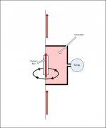
When you try to look at time varying current through a resistor, you use a pair of wires. Those wires form a loop next to the physical body of the device, and that loop will intercept the magnetic field that goes around it.
At DC, this is a 4 wire, or kelvin connection, and give good accuracy. But when the current changes, the loop area can generate a voltage based on faraday's law of induction, V =-db/dt (b-dot) times the area. (the actual field falls as 1/r, but that's not important to this discussion).
No matter what you do to a resistor internally, there will always be a physical distance between terminals, and that's where the voltage pickups have to go. I have drawn a diagram to illustrate this. The loop area is the pink hilited area, it is formed by the resistor and the wires to the scope.
My interleaves resistor design brings the current back through the body in the same path as the original current, so the magnetic field will be of the opposite sign, which causes a cancellation of the magnetic field that will be trapped in a loop.
For this EDM thing, I realized that I do not have to electrically connect the two resistors at one terminal as per my original design, but can make both to interleave nonetheless.
The result will be, both the .05 ohm and the 20 ohm resistor will have it's magnetic field cancelled by the current of the other. edit: this reduces the error I will see in the very low value current viewing resistor, and as an added bonus, it reduces the inductance of the overall loop between the fet switch, the capacitor, and the edm device, which will allow the current to rise that much faster.
The only caveat I see is any current which flows from the mechanical equipment to ground will not cancel through the resistor. This means I have to keep the capacitance to ground to a minimum.
edit: This problem is most apparent when the resistor being used is very low resistance. Then the IR drop is very small, and the b-dot error can be large with respect to the actual IR. If the resistor has a high value, then the b-dot error may be insignificant. At first blush, one only needs to know the value of the resistor's inductance to calculate the basic b dot error, v = L di/dt, then review it's level with respect to the actual IR drop.
jn
Attachments
Last edited:
A transient pulse has the high freq travelling on the outer edge where the equivelant L is lowest. In sine wave use, such as a RF signal (carrier) you dont see much affect... but with data signals it can be a disaster to the waveform fidelity. It can lead to corruption or loss of data.
THx-RNMarsh
Hence the need to pick a rise time for digital signals that is not to extreme for the signal fundamental clock frequency. Somewhere I do have some more notes on this, the other problem is trace/wire resistance varies with frequency as you get into the higher frequencies. Not to much of a problem for most digital stuff with todays clock speeds and rise times, but as clocks and more importantly signal rise times increase signal integrity issues are increasing, further influenced by the proximity of the return layer (usually a GND plane next to the signal layer). I am curious as to whether my signal integrity simulation tools take this into account, something I will look into when I get time.
Sorry, it was a long time ago. I think I had Googled for something like "anomalous skin effect" or perhaps "nonlinear skin effect". I seem to recall that the paper was referring to very high currents (or maybe high static magnetic fields?) under cryogenic conditions - I can't remember what the conductor was. The medium then became somewhat nonlinear. I am not a solid state physicist so I didn't really take much notice except to reassure myself that it was not relevant to our discussion.jneutron said:You've peaked my interest here, I'd be interested in what you found, as cryogenic stuff is part of my day job..
- Status
- Not open for further replies.
- Home
- Member Areas
- The Lounge
- John Curl's Blowtorch preamplifier part II