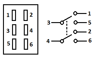
Not really - in both cases the center pins will connect to the bottom pins. And as there's nothing on the top pins, the switch still does its job.
If you wire it as in the photo, the top pins will not be hot when the switch is in the off position, so there's no issue if a microscopic metal robot enters your amplifier and crawls around the switch.")
If you wire it as in the photo, the top pins will not be hot when the switch is in the off position, so there's no issue if a microscopic metal robot enters your amplifier and crawls around the switch.
Sorry for being... childish.
I was trying to say: the switch toggles between pins 1+2 and 5+6 . Did I understand it correctly?
I was trying to say: the switch toggles between pins 1+2 and 5+6 . Did I understand it correctly?
If I get it right, that means that of those microscopic robots would fart electrons into Pin 1 and/or 2, I would hear ist through my speaker (given the quality of ACA and my understanding of the switch) ? [emoji4][emoji56]
No.
If you connected the DC power from the barrel connector to pins 3&4, when the switch was in the off position, pins 1&2 would have the power on them. As those pins are not connected to anything, it actually doesn't matter.
If the power is connected to pins 5&6, and the power taken from 3&4, pins 1&2 are never used and never connected.

After a pause I'm back at my troubleshooting. I'm the guy who has something going on that's causing the LEDs to blink. I did figure our that it's only when the right channel's V+ is connected that the blinking occurs. I unscrewed the boards to see if there is an obvious problem. I'm a novice at soldering so there some cases (like Q4) I soldered from the bottom of the board since the spacing was so tight. Can that cause issues?
I have attached two better images of what appears to be the bad (right) board. Does anyone see any problems with any connections?
I have attached two better images of what appears to be the bad (right) board. Does anyone see any problems with any connections?
Attachments
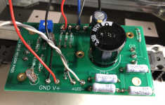
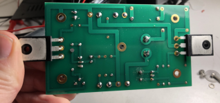
You where supposed to solder everything from the bottom except the main transistors and the cabling which you do carefully from the top. So no problem soldering on the bottom. Try going over the bottom with the soldering iron - it could be some of the joints on top only look OK. They look a little heavy like you added solder till you thought you had enough rather than wait for the heat to get in and leave you with volcano shaped joints. Fingers crossed for you - they sound excellent once done . Worth persevering with.
Hi bobertbk,
There is nothing obvious on those pictures to cause a short or to make the LEDs blink. Unless one of the joints was / is long enough to touch the chassis when the board is installed. The joints are suspect in lots of places, as has been mentioned a few times, you will need to correct them, but they are not causing the blinking problem.
In your original post you said you had smoke.
Can you recap a little please?
Is this the board that you had smoke from in your original post? Is this the 'cold' or 'hot' board?
Then please give us some resistance readings from the bad board. Use the troubleshooting section Step 56 of the build guide.
Please Do not switch the unit on with the board off the chassis or you will fry Q1 and Q2.
There is nothing obvious on those pictures to cause a short or to make the LEDs blink. Unless one of the joints was / is long enough to touch the chassis when the board is installed. The joints are suspect in lots of places, as has been mentioned a few times, you will need to correct them, but they are not causing the blinking problem.
In your original post you said you had smoke.
... When I finished all wiring and turned it on one of the transistor sets got very hot very quickly and there was a bit of smoke. ... Did I fry something?
Can you recap a little please?
Is this the board that you had smoke from in your original post? Is this the 'cold' or 'hot' board?
Then please give us some resistance readings from the bad board. Use the troubleshooting section Step 56 of the build guide.
Please Do not switch the unit on with the board off the chassis or you will fry Q1 and Q2.
Done!
I'm through!
My ACA is playing music!
It was so insightful fun! Almost sad it's already over.
There are a few questions left though:
I connected my mac through a Herus DAC, play music with iTunes/Music (output controlled by bitperfect), and there's a constant hiss, audible when the music is quiet... could it just be the setup, or something inside? (Haven't measured anything except the bias (11.9 - 12.0 v left, 12.0 - 12.1 v right)
And, I think I'll do just a second ACA, for the fun, the experiment, and the mono block. While building, I often was confused by the PCB's being identical. Building one channel upside-down to have a symmetrical layout in the chassis should work, shouldn't it?
here's some images:
The sharp-eyed observer will see that I had to solder a extension to the power-cables...
I'm through!
My ACA is playing music!
It was so insightful fun! Almost sad it's already over.
There are a few questions left though:
I connected my mac through a Herus DAC, play music with iTunes/Music (output controlled by bitperfect), and there's a constant hiss, audible when the music is quiet... could it just be the setup, or something inside? (Haven't measured anything except the bias (11.9 - 12.0 v left, 12.0 - 12.1 v right)
And, I think I'll do just a second ACA, for the fun, the experiment, and the mono block. While building, I often was confused by the PCB's being identical. Building one channel upside-down to have a symmetrical layout in the chassis should work, shouldn't it?
here's some images:
An externally hosted image should be here but it was not working when we last tested it.
An externally hosted image should be here but it was not working when we last tested it.
An externally hosted image should be here but it was not working when we last tested it.
The sharp-eyed observer will see that I had to solder a extension to the power-cables...
Ok. I wish I had read that last post before testing since I did detach the left (hot) board from the chassis to solder some of the connections under the board and then turned it on. The Q1 and Q2 did get blazing hot. I'm not sure if I destroyed them.
In any case I left the right board attached to the chassis and took all resistor and Q readings with the board facing me (R1-R4 closest to me). I recorded either the top/bottom or left/right resistor reading, depending on its orientation. You can see the results in the attached image. Many strange readings.
R11, R12, and R14 are particularly strange because the reading isn't stable. I indicated the voltage as 8* because it seemed to bounce between 6.5 and 10 or so.
Attachments
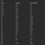
bobertbk, question - where did you put your Negative meter lead to take the readings?
Yes some of those readings are strange, Q1S for instance is (should be) connected to the GND / 0 volts track, so cannot measure +24 volts, it should be 0 volts...
The resistor R9 is also (should be) connected to the GND track, so also should measure 0 volts where you have 9.9 volts. The 4.5 volt reading is reasonable.
Same again for R14 which also has one end connected to the GND track... you should not measure any voltage on either end.
So you either have a bad connection somewhere, likely to do with the 0 volt lines, or possibly you have a wire strand, solder blob or lead touching or bridging?
The other readings (apart from the R11 and R12 ones, which will be due to what ever is causing the the R9 /14 problem) look within a working range.
Basic understanding: bias
Hello again.
I begin to slowly develop a very basic understanding of what I built. But many things are still a big ?... like the bias (no, I get what the bias is, but not in its depth. So:
What happens if I lower the bias to, say 10V? Nothing except that the amp starts to clip earlyer? And gets a bit less warm?
Thanks to all of you!
David
The heat dissipation should stay the same if you alter the midpoint voltage (bias is misleading because so many immediately think of quiescent current adjustment here).
With the midpoint set accurately each transistor dissipates the same power. If you alter the midpoint to say 6 volts then one transistor will dissipate much more power than the other due to the different voltage now dropped across each device. The current flow is unaltered.
The one with least voltage across it will be cooler. The total power dissipation of the two devices added together remains the same.
C1 Positive and Negative
Here is a stupid question that I have looked all over for, and the feedback is too general for me to act. Also, the ACA 1.6 build guide is extremely vague.
Which are the positive and negative leads on the C1 Cap? There is a Neg marker on the label but it is offset. Also one of the leads has a stamp that means something.
Unless I am missing something, which is highly possible, this is a really severe oversight in the build guide not to clearly (REALLY CLEARLY) let the person tell which lead is which. The other Caps are no problem - long lead is positive.
Thanks so much.
FRC
C1 Positive and Negative
Thanks so much. This solved it for me.
The wrapper identifying the negative on a large cap should not be offset enough to cause confusion... maybe a picture of your actual cap might help.
Thanks so much. This solved it for me.
 that's good.
- Home
- The diyAudio Store
- Amp Camp Amp Kit 1.6/1.8