From my exprience the most important factor in good listening exprience is listening to a amp that has the top amplifier schematic.The other 3 factors which affect the listening experience are - liquor, lighting, and ladies
I tried poor amp circuit with big caps and regulated supply, not much diffrence in sound what so ever.
Poor amp with good speakers when my top amp broke down due to using fake transistors. Wanted to stop listening to music cause the sound quality is soo poor with brought amplifiers.
Depends on the pass transistor and current source. Max current is when the opamp doesn't take anything from the cs and all the current goes into the base, then max output current is Ib*Hfe.
But at that point the regulation is zero of course.
And as you say, take care of the heat!
3-4A is not realistic.
Jan
But at that point the regulation is zero of course.
And as you say, take care of the heat!
3-4A is not realistic.
Jan
Versions that use a power MOSFET as a pass element have no base current limitations; they are limited only by power dissipation. The MOSFET based regulator I built (using my own PCB design, not the DIYA board!) included an Aavid 530002 heatsink (link) which rises 60 degrees C above ambient when dissipating 20 watts. If Vin is 6 volts above Vout, it can happily pass 3.3 amperes.
But did I actually operate and measure my voltage regulator board at Iout=3.3 amperes? Heavens no. I only specified "1 oz" copper thickness when ordering the PCB, and I didn't design the traces or the pads and holes, with anything more than ~ 1 ampere in mind. And in fact I only planned to use the regulator in equipment whose draw is less than 900 mA. To run at 4 amps all day long, I'd recommend building the same circuit on a brand new PCB layout with brand new connectors and "2 oz" copper thickness.
But did I actually operate and measure my voltage regulator board at Iout=3.3 amperes? Heavens no. I only specified "1 oz" copper thickness when ordering the PCB, and I didn't design the traces or the pads and holes, with anything more than ~ 1 ampere in mind. And in fact I only planned to use the regulator in equipment whose draw is less than 900 mA. To run at 4 amps all day long, I'd recommend building the same circuit on a brand new PCB layout with brand new connectors and "2 oz" copper thickness.
Actually the MOSFET regulator is much faster than the BJT version using the Jung/Didden choice of BJT (D44H11). The MOSFET's fT is about 300 MHz while the D44H11's is 40-75 MHz depending on whose datasheet you consult. Minimum permissible (Vin - Vout), a/k/a Dropout Voltage, is indeed higher in negative-output voltage regulators, because there are no depletion mode P channel MOSFETs. PSRR is mostly a function of the error amplifier rather than the pass device, but the shrewd play for those concerned about HF PSRR is to install an upstream LPF; attenuate high frequencies before the voltage regulator itself. It's just a few passive components.
Building a positive version and need some help with calculating the R6/R7 resistor values.
Input voltage is 12Vac and desired output voltage is 8V. I´m using the LM4040-5V as vref. What should my R6/R7 value be?
(8-5)/5.
I'll send you one in the mail if you promise to measure it side-by-side with a Super Regulator and report the measured bandwidths. Schematic here. I think D4 and R10 might be somewhat novel; they increase the PSRR of the reference voltage by an additional 1000X at the mains frequency, yet the extra cost of those two components is quite low. Replacing R10 by a JFET or an LM334 might get another factor of 10-30X.Mark, how much faster, any figures?
D4+R10 have been around for as long as I have been able to read regulator schematics, more than a couple of decades.I'll send you one in the mail if you promise to measure it side-by-side with a Super Regulator and report the measured bandwidths. Schematic here. I think D4 and R10 might be somewhat novel; they increase the PSRR of the reference voltage by an additional 1000X at the mains frequency, yet the extra cost of those two components is quite low. Replacing R10 by a JFET or an LM334 might get another factor of 10-30X.
Can't you add a extra common collector inseries with the cs, then you'll have max output ib*hfe1*hfe2Depends on the pass transistor and current source. Max current is when the opamp doesn't take anything from the cs and all the current goes into the base, then max output current is Ib*Hfe.
But at that point the regulation is zero of course.
And as you say, take care of the heat!
3-4A is not realistic.
Jan
Can't you add a extra common collector inseries with the cs, then you'll have max output ib*hfe1*hfe2
Yes there are many ways, but this has the big disadvantage that at light loads the opamp cannot absorb all of the current so you hit a limit there.
You can also use a darlington for the series pass device, but that adds loop gain and you probably get into oscillator-land.
Selecting the best solution and working out the new system is called, unsurprisingly, electronic design ;-)
Jan
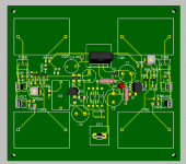
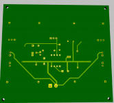
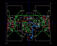
Jan ,made some changes after discussing B1 at passlab thread. Added SOIC option. Please take a look and see if there any glaring issues.
I might make a few changes, nothing critical, except one I recommend. Place the pass transistor symmetrical between the caps. That gives the best distance to either cap for heat and leaves the max space for a heatsink.
Jan
You are mistaken. What is shown is a two stage shunt regulator. The first stage consists of a current source and zener diode, having a line rejection @ DC of about 80 dB. The second stage consists of a resistor and LM329 precision reference IC, which adds another 60dB of line rejection @ DC. I very much doubt that you can exhibit a >20 year old schematic containing a cascade of two shunt regulation zener_diodes/ICs, in which the first shunt regulator is biased by a current source and the second is biased by a resistor.D4+R10 have been around for as long as I have been able to read regulator schematics, more than a couple of decades.
_
Attachments
So you mean that you can create speed with a 13 nF input capacitance mosfet?
Let's calculate the input capacitance of an (fT = 75 MHz) BJT operating at 160 mA of collector current
Cpi = gm / (2 * pi * fT)
At 160 mA **, gm = 6.2 siemens, thus Cpi = 6.2 / (6.28 * 7.5E7) = 1.3E-8 farads = 13 nF
** and at 300K junction temperature, such that the thermal voltage (kT/q) is 0.026 volts
Last edited:
- Home
- The diyAudio Store
- Super Regulator