Just directly wired the sense connection on the supperreg board to the -12V pin on the DAC IC ==> ZERO effect on the scope. Positive thing about this test is that it gave me more confidenence in the pin connectiors.
Removing the DAC from the bottom board and restively loading the suppereg's via the pin connectors removes the oscillation.
Removing the DAC from the bottom board and restively loading the suppereg's via the pin connectors removes the oscillation.
Load is 31mA for the -12V regulator.
Test: I added a Pana FC 35V 47µF parallel to the 100n decoupling cap ==> oscillation amplitude reduced from 100mVpp to 15 mVpp. Need to order some Panasonic Polymer caps (https://www.mouser.be/ProductDetail/Panasonic/20SEPF120M?qs=OE1iw1LrrPGaVmyWj69G7A==)
Test: I added a Pana FC 35V 47µF parallel to the 100n decoupling cap ==> oscillation amplitude reduced from 100mVpp to 15 mVpp. Need to order some Panasonic Polymer caps (https://www.mouser.be/ProductDetail/Panasonic/20SEPF120M?qs=OE1iw1LrrPGaVmyWj69G7A==)
Last edited:
It's most probably the high-Q ceramics on the DAC board.
The final cap on the superreg board should have non-zero ESR to provide enough damping.
The idea is that with a bit of (inductive) wiring between the superreg board and the load (here the DAC) there would be sufficient isolation between the superreg and whatever is at the load.
With directly plugging the reg boards to the DAC/motherboard that isolation isn't there.
To verify that the diagnose is correct you could temporarily remove the 0.1u ceramics at one of the loads and see if the oscillations stop.
If that is the case we need to come up with a solution ...
Edit: where did you add those elcaps? At the superreg out or on the DAC board?
Idelly as far away as possible from the superreg, like after the headers, close to the DAC.
Jan
Last edited:
Yes, the elcaps are placed close to DAC pins. As far as possible from superreg out.
Directly at the superreg out, there are high ESR tantal caps (6ohm at 100kHz): https://www.mouser.be/ProductDetail/KEMET/T491A475K025AT?qs=%2Bcwu2E9E7oWIZoJQLPvDlQ==
I removed the 100n COG decoupling caps from DAC pin's ==> result is back to 100mvPP oscilation.
Remark: the 10R sense resistor is bypassed, the 10 cap at superreg board is removed.
6 ohms is pretty high, maybe too high.
I always tested with less than 1 ohm.
Edit: when you say " the 10R sense resistor is bypassed, the 10 cap at superreg board is removed." , is the sense directly conneted to the force pin, directly at the superreg board, not going through the header?
Jan
I always tested with less than 1 ohm.
Edit: when you say " the 10R sense resistor is bypassed, the 10 cap at superreg board is removed." , is the sense directly conneted to the force pin, directly at the superreg board, not going through the header?
Jan
Wait a minute..., I see big differences when holding the scope probe by hand or clamp it on a wire without touching the probe. I'm afraid I need to do the entire exercise over.
Jan, on the superreg board is mounted the tantal as mentioned in post 3447. on the main board, on which the superregs are placed, a 100µf 35V Nichicon FG is there (20mm from the superreg PCB). In my understanding, both are low ESR. The tantal is there, just for stand alone testing of the superreg's.
The trace lenght between superreg and load is approx 60mm.

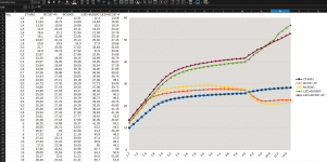
I've tried to make a structured overview with all tested parameters and the result.
Quite some things can be concluded out of this for my next PCB revision.
I quickly tested an LM7912 as well. Compared to my PCB layout of the Jung-Didden, the amplitude of the oscillation was smallest.
I'll ask in the AD1862 Miro Thread of someone can make me a scope shot.
Quite some things can be concluded out of this for my next PCB revision.
I quickly tested an LM7912 as well. Compared to my PCB layout of the Jung-Didden, the amplitude of the oscillation was smallest.
I'll ask in the AD1862 Miro Thread of someone can make me a scope shot.
Attachments
Yes indeed, same frequency.
I gave up and inserted an inductor in the psu traces (out of the feedback network with the sense connections). Inductors are 47uH (RDC about 6 ohms ☹️). Oscillations are completely gone.
Now, what is the added value of using these Jung-Didden superreg’s in this configuration with the inductors?
So yes, nothing wrong with the regulators, just a PITA load.
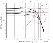
Having encountered strange behaviour at high load and minimum voltage offset, i decided to compare input CCS stability with dual BJT vs LED+BJT at different VCC levels, as in super regulator , Voltage offset is the VCC for CCS. I loaded the CCS with one silicone diode drop to simulate pass transistor. I tried to be as scientific as i could be for 1 hour, first 4 Volts in 0.1V steps, from 4 to 15V in 1V steps, all other elements unchanged.
It seems, that at high current draw i get too much voltage drop on input cables from PSU, thus lower input voltage. Having too low input voltage, results in simultaneous VCC drop for CCS (i.e. regulator offset), and while CCS current input droops, the pass transistor being in it`s own beta droop region, needs MORE current. Last night i was able to get to 0,93 Volts offset with Vout stable at 0 to 1 Ampere draw, but it seems that at this offset, my input CCS is already giving it`s lats few mA, while pass transistor is still able to keep up with regulation, while op-amp does it`s magic.
Input CCS stability chart shows, that much cheaper and widely available BC337_40 at low offsets is actually more stable than expensive and momentarily unavailable ZTX851, to my relief. Also dual BJT CCS seems a better choice than BJT+LED at low input offsets, but in general a minimum 2 Volts offset seems most advisable if I want to count for input voltage drops at sudden current draws.
Attachments
Yes indeed, same frequency.
I gave up and inserted an inductor in the psu traces (out of the feedback network with the sense connections). Inductors are 47uH (RDC about 6 ohms ☹️). Oscillations are completely gone.
Now, what is the added value of using these Jung-Didden superreg’s in this configuration with the inductors?
So yes, nothing wrong with the regulators, just a PITA load.
Which hints the datasheet spec of a 0.1 uF capacitor is lower than it should be. I'll ask a silly question: are you sure that's a C0G and not an X7R or something else in the circuit? If it is, then perhaps a heftier part in X7R rated to 50 volts or above could do the trick. Non-C0G ceramics tend to lose capacitance when biased, with the effect reduced at voltages less than rated, hence the >50v recommendation. Mouser is crawling with 1206-sized 4.7 uF at 50 volts so choice isn't an issue.
I'll also bet the 100uF 35v electrolytic is a low-ESR type, in which case you could have a parallel resonant tank with the bypass ceramic. Electros of that size tend to have equivalent inductances around 100 nanoHenries, so with 0.1 uF in parallel the resonant frequency would be not far from 1.5 MHz, and a bit of PCB trace inductance could bring that down around 1 MHz. Remember Q = (1/R) * (√(L/C)), so with L close to the same magnitude as C then Q ~= 1/R, hence the tank would have a Q of 5 with a cap featuring 200 milliohms of ESR.
Looking at the bypass impedance, a simple model of the electrolytic impedance as Zce + ESR + ESL says the capacitive contribution is nil at high frequencies so at the frequencies of interest its form is ESR + ESL. Plugging that in the parallel equation with the ceramic as Zcc, the impedance becomes ((ESR + ESL) * Zcc) / (ESR + ESL + Zcc) and at resonance it simplifies to ((ESR + ESL) * Zcc) / ESR since Zcc and ESL cancel each other in the denominator. With the values shown above the bypass impedance rises from 200 milliohms, as contributed by the electrolytic somewhat below resonance, to 5 ohms at the resonant peak. Active devices switching quickly could excite that resonance, bouncing the supply rail.
Replacing the specified 0.1 uF capacitor with a 4.7 uF ceramic sorts that out nicely since its resonance with the same electrolytic would have Q at a more reasonable 0.7, causing barely a ripple in the bypass impedance.
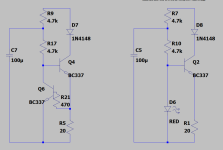
Quick question about the led's in the standard version of the super reg: currently I'm building one with a red led for the neg reg and a green led for the pos reg. Vf for the red is 1,8V, for the green 1,95V (measured). Does this difference have any consequence for the functioning of the super reg (bias for Q2 and Q4?)
I have a question about my +30V version of this regulator using my own PCBs. From this batch of PCBs I have built both +13V and +20V successfully at the first try. They are dead on and completely stable. Very nice.
The +30V unit won't work. The output measures at around 26.7V and it is not stable. In a range of several tens of mV it hovers around that value. Like it's not going into regulation. The LED is giving off light like it thinks it has to light up the entire room - way more current is flowing through it than I'd have expected based on the light coming off the 13V and 20V units that work perfectly.
Is the current sink part of the circuit not working properly at this voltage or because of some other reason?
I am using:
Opamp AD825
R6 1.78k
R7 562R
D2 is a 15V zener (1N5245)
Vref is LM329
My electrolytic caps are 100µF/50V Panasonic M, as far as I can tell a general purpose cap with an ESR that's not very low.
The input voltage from the rectifier is a bit high: 40V. The 20V unit that I got working takes 30V from the rectifier, so the 10V drop seems in principle unproblematic.
Otherwise it's built in accordance with Jan's instructions in the DIY Audio Store, except for R2 which I doubled as the 40V unregulated input rail woud in theory make the LED shine a bit bright. (Which it now does anyway.)
Until now I have only visually checked the board and components with my 15x goggles, making sure no immediately apparent mistakes are there. (Like I once soldered the AD825 in the wrong orientation, any short circuits of component leads, having used the correct values in the correct places, that sort of stuff.) I triple checked the wiring, making sure there was continuity in the right places and not the wrong ones. I tested the unit with a 1k resistor as the load, with sense lines connected. The LM329 is functioning like it should, measuring at a steady 6.90V when the circuit is powered up.
Is there anything about a 30V super regulator that should be changed from the instructions?
The non-inverting input seems OK-ish with the ref diode being nominal 6.9V
The midpoint of the resistor values times Vout seems too low.
What are the resistor values? Is that correct to divide down the target Vout of 30V and end up at 6.9V?
Take R6/R5, plus 1, times Vref of 6.9. That's about what you have. So the error is clear.
Jan
The midpoint of the resistor values times Vout seems too low.
What are the resistor values? Is that correct to divide down the target Vout of 30V and end up at 6.9V?
Take R6/R5, plus 1, times Vref of 6.9. That's about what you have. So the error is clear.
Jan
- Home
- The diyAudio Store
- Super Regulator