Yes, pin 1 and 2 are together. Pin 3 and 4 are together. Not connected to the pos reg board for testing. Any other ideas?Did you connect the remote sensing on J4 - For testing - pin 1 and 2 And pins 3 and 4
A CCS is a 2-terminal device, so you can just flip it around. Only the relative polarity at the two terminals needs to be correct.Thank you, grunf. They will be for GLED431 CCS, as I understood 5mA for it is enough? GLED431 should replace LM329 6.9V voltage reference in Jung/Didden Superregulator. Now I am trying to understand how to revers it for negative -15V supply.
View attachment 1244346
Jan
I found the mistake, I had somehow Q4 emitter to the ground without resistor. My own pcb mistake.
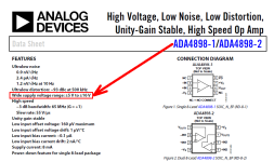
So far I still do not have figured out this ADA4897 issue. With OPA1641 I have output 17 volts (I can change output value) and when I but ADA4897 then output is 6.5 volts. I am using variable resistor for R6. Changing resistor R6 value it does not change voltage. Any thoughts about this?
So far I still do not have figured out this ADA4897 issue. With OPA1641 I have output 17 volts (I can change output value) and when I but ADA4897 then output is 6.5 volts. I am using variable resistor for R6. Changing resistor R6 value it does not change voltage. Any thoughts about this?
i must report, that op-amp ADA 4898-1 gave me excellent results with standard schematic from Jan. I found this op amp on other forum, where somebody described them as "AD797 done right". Noise figures on datasheet are as good as AD797, but gain curve shows even higher OLG at higher frequencies than OPA1611 or AD797. Internal compensation cares for phase margin, and my prototype board REFUSED to oscillate with pulling every capacitor out, till i took out the last cap across 4 and 7 of the op amp itself. Then i saw on the scope a short burst of violent oscillation, and shortly after ADA4898-1 in soic to dip adapter exploded melting the adapter. 🙃
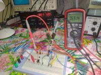
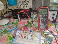
As for GLED431, in my case a series of four HLMP 6000 with 24 Ohm trimmer resistor plus ZTX951 with 220 Ohm E to B, show me 6,912V on my Brymen 869s. 20 Ohm resistor would be closer to the lm329. I measure around 2,6 mA in the LED branch, and 5,1mA in the ZTX951 branch from BSS139 biased with 100 Ohm (7,76mA CCS, 100R is convenient point for measurements as well). Vref stays very stable with Vin from 12 to 32V, more harm causes just waving my hand over board than changing Vin by 20volts. Rising the temperature with hot gun lowers Vout, which gives a weak temperature negative feedback effect for my class A amplifier.
As for GLED431, in my case a series of four HLMP 6000 with 24 Ohm trimmer resistor plus ZTX951 with 220 Ohm E to B, show me 6,912V on my Brymen 869s. 20 Ohm resistor would be closer to the lm329. I measure around 2,6 mA in the LED branch, and 5,1mA in the ZTX951 branch from BSS139 biased with 100 Ohm (7,76mA CCS, 100R is convenient point for measurements as well). Vref stays very stable with Vin from 12 to 32V, more harm causes just waving my hand over board than changing Vin by 20volts. Rising the temperature with hot gun lowers Vout, which gives a weak temperature negative feedback effect for my class A amplifier.
Attachments
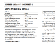
What a surprise. Nobody here did not mentioned that max op amp voltage for this ADA 4898-1 is 11 volts. My input voltage is higher than that. Does that mean that I have to say goodbye to this ADA 4898-1 and to buy new after I have tested it with a higher voltage like 20 volts?ADA4897 has 11V max supply voltage, that's why it doesn't work properly.
ADA4897 is a great choice for 5V output reg.

Ada 4897 and ada4898 are two different parts, and i found it a good practice to simulate first in ltspice every new idea, check the nodes for voltages and elements for power dissipation, checking simulated values against max values in datasheet, then building on prototype board, measuring and comparing prototype to simulation, and only then ordering new PCBs. It's is advisible to stay in a healthy distance from max declared values. And pay attention to every little count in part number, as sometimes it becomes something entirely different and stops your PCB from working entirely, even though 4897 and 4898 may seem similar numbers. I aim for 22vout and 4897 will be destroyed here. For lower vout 4897 may be better.
Last edited:
addendum to GLED431 from post 3426.
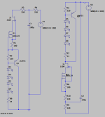
Bypassing the j109 and letting bss139 run on it's own, makes no difference to the Vref stability, i.e. it changes 2mV / 20V. Nmos sees higher VDS change, but is in higher more stable VDS region from the start, so net effect is the same, with one part for cascode spared. CCS stability without cascode is worse by 0,2mA / 20Vin, and it can be pure thermal effect of higher power dissipation bss139, but it doesn't seem to bother the GLED431. I don't expect any AC voltage from super regulator output, and 2x220R+100uF on the Vref input is paranoidal enough.
Changing the 24Ohm R that i had at hand to 20 Ohm, made Vref 6.905, comparing to lm329 sample 6.901, which allows me to make direct swap comparisons after Christmas, without worrying that a miniscule change of rail voltage would turn my sound impressions upside down.
Small question before cutting traces on my pcb.
I’m feeding my ad1862 DAC (all 4 voltages) with Jung-Didden supperregulators. Worst case oscillation I measured, on one voltage was 40mvPP @ 1.x MHz. I’m using the sense option including the 10R + 10n trick.
question: does is make sense to add an inductor in the output trace of the regulator BUT before the sense connection, this to compensate for the dcr losses in the inductor?
If you do that, you add the inductor inside the feedback loop.
It's questionable whether that cures the oscillation, it might as well increase it.
Can you give some info on the oscillating regulator?
Any differences with the stock unit, which opamp, what output capacitor?
Jan
It's questionable whether that cures the oscillation, it might as well increase it.
Can you give some info on the oscillating regulator?
Any differences with the stock unit, which opamp, what output capacitor?
Jan
Dag Jan,
Ok, thanks for the feedback.
My situation:
1. LM317 preregulator with output 18V for the 12V JD regulator.
2. +- 10cm of wiring to PCB on which Jung-Didden superreg's are placed on using pin connectors.
3. Superreg's output voltages: +5V -5V, +12V, -12V. AD825 opamp for 12V and AD817 for 5V, output cap = tantal (Mouser 80-T491A475K025AT) followed by a Nichicon FG 35V 100µF. Both not low ESR in my understanding.
4. AD1862 pcb stacked on the above mentioned PCB. 100nf COG's decoupling direct on DAC pins.
Other info.
The same Jung-Didden reg's are used on the IV-stage. Probing here shows a flat line on the scope. (visual no difference when probing the ground).
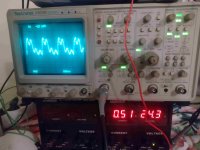
Oscillation on the +12V and -12V is a factor of 2 higher in amplitude than the +5 and -5V. -12V = 100mVpp @1.04MHz (rechecked today.
Regards
Ok, thanks for the feedback.
My situation:
1. LM317 preregulator with output 18V for the 12V JD regulator.
2. +- 10cm of wiring to PCB on which Jung-Didden superreg's are placed on using pin connectors.
3. Superreg's output voltages: +5V -5V, +12V, -12V. AD825 opamp for 12V and AD817 for 5V, output cap = tantal (Mouser 80-T491A475K025AT) followed by a Nichicon FG 35V 100µF. Both not low ESR in my understanding.
4. AD1862 pcb stacked on the above mentioned PCB. 100nf COG's decoupling direct on DAC pins.
Other info.
The same Jung-Didden reg's are used on the IV-stage. Probing here shows a flat line on the scope. (visual no difference when probing the ground).
Oscillation on the +12V and -12V is a factor of 2 higher in amplitude than the +5 and -5V. -12V = 100mVpp @1.04MHz (rechecked today.
Regards
Attachments
@Bensen It sure would be nice, if this type of question could be answered remotely, but I'm afraid there is no way around building an actual prototype with real world elements and checking out for yourself. I get similar type of oscillations after at different load levels, but no one on this forum can put the base resistors and make measurements for me. Put a coil and see what happens, you might find something inspiring for next project. All i wanted was put a faster smaller pass transistor the 2sa2222sg (thanks Mark Johnson!) , and use constant feedback CCS from dual bc337-40 on the input (Mark Johnson again with his low semi saturation transistor thread). Under certain load level, i see this mess now. It stabilizes only when i load with over 3.6A now, under that i see 40-60mV at 6,8MHz. No matter how many questions i write here, nobody puts for me some base resistor and/or input capacitor, so i guess i have to do it all myself..
Attachments
![IMG_0411[2].JPG](/community/data/attachments/1159/1159418-2948ce4402ffa841f4a71c1e116d877d.jpg)
when i played with diffrent LED colors on input CCS, I noticed it had affected the minimal voltage offset.
I decided to use ANF CCS type with dual BC337-40 from Onsemi on the input in hope to minimize the offset for high current class A.
Active load gives me some messy measurements, i had to switch to non inductive power resistors.
With dual BC337 I can go down to 1,31V minimum voltage offset under heavy load, i.e. i can go from 0 to 3.3A with no detectable change of output voltage.
With 20 Ohm CCS programming resistor i see 30mA input current, which with the 2SA2222SG allows for max 4.9A regulation. Max Dissipation 4.9x1.31 = 6,42 Watts, the TO220F package on small Avid heat sink reaches 60 Celsius at the screw, well below max allowable ratings for this relatively small pass transistor.
The only thing that worries me is that i see some very small "oscillations" all the time, like 6mV pp of some irregular shape, i don`t know if it is even an oscillation, or i just pick up some wifi with this cable salad.
One more important thing i noticed is, that counterintuitively, low ESR at the input of superregulator makes response to square wave load worse and oscillatory, but again it can be the fault of Zhaoxin PSU and long cables. I`ll try tomorrow with an SMPS from MeanWell that will be used in the endproject, as it showed a better transient regulation than all other sources, and then again how it all fares with CLC filter in between.
Attachments
Last edited:
Low ESR making regulators ring a little bit is not insane. For example, LM7915s are notoriously prone to oscillations when the outputs are bypassed with ceramic capacitors instead of the tantalums recommended on the data sheet, and some problems with the LM7xxx series can be tracked down to the regulators interacting with the obligatory 0.1 uF opamp bypass caps. Amusingly enough, skimping PCB trace width introduces a little bit of resistance and inductance which helps the matter slightly.
Wayne Colburn kicks it up a notch with 47 ohm resistors between the regulators and opamp rails, which might seem excessive until one considers that opamps eat a few milliamps so the voltage drop is a fraction of a volt. Also (a little secret) the characteristic impedance of a 1/8 inch (3 mm) wide trace over a ground plane on the other side of a 1/16" (1.5 mm) board is ... drum roll please ... 47 ohms! Now why is this important? PCB traces are maybe a few inches long so why would matching impedance concern us at audio frequencies? The answer: trace VSWR is unimportant at audio frequencies but it does become an issue when considering immunity from RF interference. Opamp PSRR decreases with frequency until falling below 20 dB above a few MHz, so a variety of far-ultrasonic grunge can enter the device through its power pins.
As a result, crapping up voltage regulation right at the opamp can have paradoxical beneficial results. Then there are other possibilities, but the margins of this post are too narrow to contain the proof...
That's hard one. So many variables with multiple units interconnected.Dag Jan,
Ok, thanks for the feedback.
My situation:
1. LM317 preregulator with output 18V for the 12V JD regulator.
2. +- 10cm of wiring to PCB on which Jung-Didden superreg's are placed on using pin connectors.
3. Superreg's output voltages: +5V -5V, +12V, -12V. AD825 opamp for 12V and AD817 for 5V, output cap = tantal (Mouser 80-T491A475K025AT) followed by a Nichicon FG 35V 100µF. Both not low ESR in my understanding.
4. AD1862 pcb stacked on the above mentioned PCB. 100nf COG's decoupling direct on DAC pins.
Other info.
The same Jung-Didden reg's are used on the IV-stage. Probing here shows a flat line on the scope. (visual no difference when probing the ground).
Oscillation on the +12V and -12V is a factor of 2 higher in amplitude than the +5 and -5V. -12V = 100mVpp @1.04MHz (rechecked today.
Regards
How/where did you connect the sense connections?
Jan
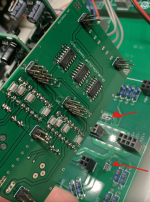
The sense connections are made on the bottom board, on which the DAC is stacked. 10R sense resistor is connected to point where PSU trace is splitted towards Left and Right DAC.
2sense resitors are on the top side, the other 2 are located on the bottom side of this PCB.
This morning I bypasses both the 10R sense resistors and the 10n cap ==> oscillation amplitude decreased slightly (-30%) on +12V, -5V and +5V. ON -12V the 100mVpp remained at about 1MHz.
2sense resitors are on the top side, the other 2 are located on the bottom side of this PCB.
This morning I bypasses both the 10R sense resistors and the 10n cap ==> oscillation amplitude decreased slightly (-30%) on +12V, -5V and +5V. ON -12V the 100mVpp remained at about 1MHz.
Attachments
- Home
- The diyAudio Store
- Super Regulator