It will be fine ") . Just need to reduce R5/R6 to 47R or less and replace BC847/857 with BCW66/68 or BC817/818.
. Just need to reduce R5/R6 to 47R or less and replace BC847/857 with BCW66/68 or BC817/818.
Increasing the current through Q1/2 will increase the dissipation in Q5/8, but this is necessary for the 1A current through Q3/4.
There are other ways but more on that another time.
. Just need to reduce R5/R6 to 47R or less and replace BC847/857 with BCW66/68 or BC817/818.Increasing the current through Q1/2 will increase the dissipation in Q5/8, but this is necessary for the 1A current through Q3/4.
There are other ways but more on that another time.
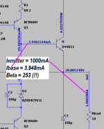
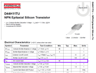
I honestly forgot about that, ty for bringing it up. The easiest solution would probably be lowering R5/R6 and swapping Q5/Q6 with a transistor in a SOT-223 package e.g. BCP-56 for better thermal dissipation. I also thought about using a darlington pass transistor, but will have to measure how stable the system is with that. Of course, using higher-beta transistors would also be doable.Looks like your circuit requires the pass transistor (D44H11 / D45H11) to have a current gain of 153 when the load current is 1000 mA. Unfortunately the datasheet only guarantees a current gain of 60. So you may have to sort your transistors by measured current gain, and discard the ones with low beta.
@BucketInABucket , I have to apologize, I neglected that you have a 1N4148 instead of a red LED, so it changes the situation a bit, here's what ltspice says, I also put dissipations on tranzistors . However, since LTspice and reality sometimes do not match, it is best to determine the value of R5/6 by experiment. In the most unfavorable case (when there is no load on the output), the dissipation at Q5/6 will not exceed 100mW.
Attachments
The simulated transistor is much much better than the datasheet guarantee. So you may have to measure your real-world transistors and sort them by current gain, then discard the ones which match the datasheet (Beta << 250) but not the simulation.
Attachments
don`t forget to include discharge resistor for the base input capacitance for the Darlington
http://www.valveradio.net/audio/darlington.html
http://www.valveradio.net/audio/darlington.html
Hello all, I hope someone can help me. I'm a valve man really, the Land Rover of amplifiers, please be gentle with me .
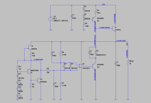
I've been learning how to use Eagle and had a go at drafting the SuperReg circuits (trust me to pick software that will be end of life soon). I've stuffed a positive board and it seems to work, though the output voltage sags for currents greater than 0.5A so I've investigated and I think the problem might be an incorrect zener for D2/6.8V.
I have a 7.5V+7.5V 75VA transformer supplying a simple LM317 reg outputting 16V. I want 12V out of the SuperReg at around 0.5A and tested with 26.8R test load with the sense wires also connected. Originally I had 15V into the SuperReg but a load of 23.4R (513mA at 12V) caused the voltage to drop to around 8.5V IIRC. Increasing the voltage in to the SR to 16V helped a little, but even taking the SR input voltage from the 21.5V on the LM317 10kuF filter wasn't much better.
Measured voltages are as below. C1-10 are 100uF, Q1 is TTC004 as D44H11 aren't available, the op amp is AD825, and R6 is 642R for 12V out.

The obvious outlier to me is the voltage drop across D2. This is what I bought from Mouser, but I'm doubting it is what it should be
6.8V zener.
I've not tested a zener before but Google is my friend. I didn't test the zener in circuit but another from the same batch - I added a 1k resistor and the zener between the return and 12V out of the load and got 0.8V across the zener. This is neither 6.8V or the 2.1V measured in circuit.
The zener doesn't look like the small picture in the datasheet, is it likely I've got the wrong part? If so I'll have to order some more as I don't have any other 6.8V zeners. Or is there something else going on that I've missed/done something dumb?
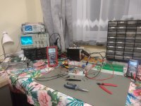
A couple of photos for reference.

The board itself - I followed Jan's layout as closely as I could. Note that Q2 is the wrong way round for the silkscreen - this is correct, somehow Eagle changed the pins I think.

Thanks,
Simon.
.I've been learning how to use Eagle and had a go at drafting the SuperReg circuits (trust me to pick software that will be end of life soon). I've stuffed a positive board and it seems to work, though the output voltage sags for currents greater than 0.5A so I've investigated and I think the problem might be an incorrect zener for D2/6.8V.
I have a 7.5V+7.5V 75VA transformer supplying a simple LM317 reg outputting 16V. I want 12V out of the SuperReg at around 0.5A and tested with 26.8R test load with the sense wires also connected. Originally I had 15V into the SuperReg but a load of 23.4R (513mA at 12V) caused the voltage to drop to around 8.5V IIRC. Increasing the voltage in to the SR to 16V helped a little, but even taking the SR input voltage from the 21.5V on the LM317 10kuF filter wasn't much better.
Measured voltages are as below. C1-10 are 100uF, Q1 is TTC004 as D44H11 aren't available, the op amp is AD825, and R6 is 642R for 12V out.
The obvious outlier to me is the voltage drop across D2. This is what I bought from Mouser, but I'm doubting it is what it should be
6.8V zener.
I've not tested a zener before but Google is my friend. I didn't test the zener in circuit but another from the same batch - I added a 1k resistor and the zener between the return and 12V out of the load and got 0.8V across the zener. This is neither 6.8V or the 2.1V measured in circuit.
The zener doesn't look like the small picture in the datasheet, is it likely I've got the wrong part? If so I'll have to order some more as I don't have any other 6.8V zeners. Or is there something else going on that I've missed/done something dumb?
A couple of photos for reference.
The board itself - I followed Jan's layout as closely as I could. Note that Q2 is the wrong way round for the silkscreen - this is correct, somehow Eagle changed the pins I think.
Thanks,
Simon.
Simon2A3 - Why did you flip Q2 ? The silkscreen should be correct.
If your using TTC004B - that is what needs to be flipped as the board is laid out for D44H11 (B-C-E)
and TTC004B is (E-C-B)
If the voltage of your D2 Zener is off a little - unlikely that is causing the problem
If your using TTC004B - that is what needs to be flipped as the board is laid out for D44H11 (B-C-E)
and TTC004B is (E-C-B)
If the voltage of your D2 Zener is off a little - unlikely that is causing the problem
Thanks dvd7900. I'd forgotten about the TTC004B pin incompatibility. I missed it when I was drafting the board but picked it up when I was stuffing the pcb. As it's a plastic part I just turned it around, but thinking about it now maybe I should have tried to mount it on the other side of the sink?
Q2 is an odd one. Originally I tried to have a positive and a negative reg in one schematic, but when I tried to add the negative version to the schematic Eagle warned me - I didn't fully understand it but I think it was warning me it was reassigning pins in the BC556 part. So I deleted the neg reg and the BC556 and reinserted, but it seems to have kept the BC546 pins. A little knowledge is a dangerous thing.
Q2 is an odd one. Originally I tried to have a positive and a negative reg in one schematic, but when I tried to add the negative version to the schematic Eagle warned me - I didn't fully understand it but I think it was warning me it was reassigning pins in the BC556 part. So I deleted the neg reg and the BC556 and reinserted, but it seems to have kept the BC546 pins. A little knowledge is a dangerous thing.
Well, I've just hooked it up to a mosfet follower headphone amp I made and wow, the improvement over the simple LM317 reg I used to get me going is so stark it's not even funny. It's like the difference between AM radio and hi fi.
But the voltage has dropped to 8.5V instead of 12V so I need to get to the bottom of this.
But the voltage has dropped to 8.5V instead of 12V so I need to get to the bottom of this.
But the voltage has dropped to 8.5V instead of 12V so I need to get to the bottom of this.
Some progress perhaps. I remeasured the voltages with the headphone amp connected and within around 10 mins Vout had sagged to 7V. I looked at the datasheet for TTC004B and wondered if I was close to the max. Collector power dissipation of 1.5W (10W @ 25C). 4V drop @ 0.5A is 2W.
I thought I had some large SK104 sinks but they must be hiding with all the other bits I'm sure I have somewhere. So I bodged a SK129 on it's side and made sure I had the back of the TTC004B on the sink this time. After an hour or so it's stabilised at 9V.
Better, but now I'm wondering just how big a sink I might need. Does this sound plausible? The boards only have provision for a smallish sink. At the moment it's on free air, if I ever put it in a case I might have to use the chassis itself as a sink.
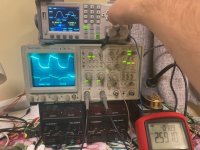
I just had a free week between projects, and spent it all doing all tests and comparisons.
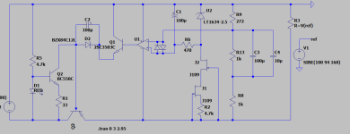
My Superreg is supposed to run from 24VDC industrial SMPS and provide at least 3A peak with minimal voltage offset.
I found a >2,5V offset a pretty safe headroom for all circumstances and load level.
For Ref i used for now TI LM 336-2.5, as i may want to go later on with Jung GLED, but don`t want to bother right now. It is RC filtered anyway (?).
I found that bypassing C1 and C3 on original schematic from Jan Didden, with a ceramic 25V 10uF, helped for better results.
I compared following op-amps i had in the drawer, AD797, NE5534, OPA134, OPA227 and OPA228.
AD797 was just a waste of time in my case, i never managed to make the Regulator stable in all circumstances.
NE5534 is doable, but does not like jumping higher than 2.4A and was sometimes a little unstable, and with longer load pulses the output voltage was drifting up and down.
OPA228 was at first most succesfull in prototype board, but had a region of slight unstability between 3.0 and 3.6 A, depending on amount of bias current from input CCS, and under heavy load or longer pulses, output voltage was drifting as well.
I`ve got best results with OPA227, which didn`t catch my eye at first based solely on "slow" specs. This op amp was spectacularly stable under all loads, held output voltage stable under longer pulses, under slow sweep from 0.001A to 4.1A (with the same bias current for all op amps above), this one NEVER showed any sign of oscillations, and showed me the best shape of output voltage from all above.
It has been a long week, but i finally found out what "unity gain stable" and "high precision op amp" mean.
I just hope, that ADA4898-1 that i ordered, will show same great results.
With some low ESR cap at the load, inductive spike is gone and with all this cable salad on the table, i got like 10mV p-p with 0 to 4.0A pulses. Is it any good ?
Attachments
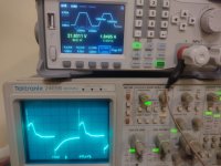
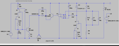
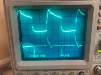
After adding RC filter for the D1 reference diode for input CCS, and a cascoded jfet CCS for D1, i managed to see 4-5mV p-p ripple with OPA227, with 0 to 4A square wave load. Upper trace is 350mV ripple from input SMPS 100mV/div, lower trace from Superreg output 5mV/div.
With capacitor on load, 3300uF/100V Nichicon, i get lower ripple, but i takes longer to get back to equilibrium, without a cap the inductive spikes are higher, but it reaches programmed voltage faster. Seems, that a 2,6V in/out offset is the sweet spot for minimal loss, and highest current available - with just 2,3 i get stable only max 3.0 A, and with 2.7 i see no further gain at 4.0A. The buffer transistor for op-amp gets hot! Choosing a 12V Zener helped, but now the diode is also very hot. I have to take it into consideration for the bypass capacitor at the Zener, as both adjacent elements are serious heat sources. Input ccs is programmed for 50mA and at 1.2A constant load desired for JLH amp, the buffer transistor for op amp conducts 28mA, which keeps the SC3503 in the highest fT zone. Discharge resistors for gates of pass transistor and buffer transistors, with best values according to theory, make no visible changes.
With capacitor on load, 3300uF/100V Nichicon, i get lower ripple, but i takes longer to get back to equilibrium, without a cap the inductive spikes are higher, but it reaches programmed voltage faster. Seems, that a 2,6V in/out offset is the sweet spot for minimal loss, and highest current available - with just 2,3 i get stable only max 3.0 A, and with 2.7 i see no further gain at 4.0A. The buffer transistor for op-amp gets hot! Choosing a 12V Zener helped, but now the diode is also very hot. I have to take it into consideration for the bypass capacitor at the Zener, as both adjacent elements are serious heat sources. Input ccs is programmed for 50mA and at 1.2A constant load desired for JLH amp, the buffer transistor for op amp conducts 28mA, which keeps the SC3503 in the highest fT zone. Discharge resistors for gates of pass transistor and buffer transistors, with best values according to theory, make no visible changes.
Attachments
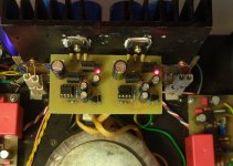
@Simulacrum, my first version whose scheme was posted by viltsone a couple of pages ago (pictured) worked quite stably with my JLH69, the output voltage was +/-19V 4A with a voltage drop of 3V on the regulators. The reference then was LM329 and op amp was NE5534.Later I replaced NE5534 with AD825.
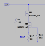
You can make a big improvement if you replace the entire input CCS with a depletion mode mosfet or even better with a cascode, I recommend BSP149 for the upper mosfet and BSS139 as the lower mosfet with the condition that you pay attention to the SOA for the lower mosfet(or use two BSP149).You can use the same CCS for LM336 in your case.By the way, GLED431 is much better than LM336 and even more expensive 2.5V references.
In my new version, I use two BSS139s set to a current of 28mA, but I only need 200uA for 2A at the output of that, the rest goes to a low-noise reference that changes the zener so that the dissipation on the buffer transistor for op-amp is only 230mW. For the buffer transistor I use 2SA1534A/2SC3940A.This is a big difference from the first version I made when I used TO220 transistors.With this solution, I can have a minimum voltage drop on the regulator of less than 2V without loss of performance.
Attachments
grunf, many thanks for your contribution in this thread, i read all of your previous posts and find them very helpful.
At the start i had difficulties to make the regulator work at all, as LTSpice can take anything, and allows to learn a lot. On prototype board it becomes a different story. After many failed attempts with too complicated CCSes and discrete references, i decided to start from vanilla and get it running first, and change bit by bit different parts, readjust CCS bias currents and try all tests, slow sweep, pulse, different offsets and so on. That is why it took me a whole week of holiday to find out , that e.g. exact level of voltage reference (be it 2.5 ; 5.0 ; 6.9) has no effect, yet good stabilization for reference and input CCS helps. And that op amp may seem stable at one load level, and become unstable, whether at different levels, or from transition, or how the internal error of op amp causes the Vout to drift. OPA227P was a revelation here. I`ve seen it on simulations before, but it`s nice to have it verified on real board. I found about infineon depletion mosfets on other thread about absolute best CCS topologies here, someone recommended exactly this line, and i have them in shopping basket. For now i just used what i had at hand i.e. j109 which is good for very small currents only.
I was thinking also about going full Darlington on pass transistor instead of buffer transistor at op amp, as it seems easier to make a high quality CCS for small currents, but it the Zener becomes a problem here - it needs more current for low noise.
BTW - 250mW at TO-126 buffer transistor and 300mW at 12V Zener is not "little", these elements are HOT, and make me worry about long time reliability of them. Some snap-on heat sink on TO-126 seems advisable, and for 12V Zener i might go with 3x3,6 in series.
Have you tried paralleling the capacitors across Zener and voltage divider in sense circuit with big mlcc capacitors ? High temp actually helps them get bigger, and they are unparalelled in terms of ESR.
It seems to my eyes, that it shortens settling time after pulse.
I did venture under 2 Volts of offset voltage to check the limits, but torture test of square wave at 4A jump showed , that going just from 2.3 to 2.6 i could get stable 4.0 instead of just 3.0Amps jump, and i decided i can loose this 0.6 V of rail for the sake of making kings and popes cry at night.
Last edited:
Your Q2 current might be too low to support enough base current into the pass device to support 0.5A output.Hello all, I hope someone can help me. I'm a valve man really, the Land Rover of amplifiers, please be gentle with me
I've been learning how to use Eagle and had a go at drafting the SuperReg circuits (trust me to pick software that will be end of life soon). I've stuffed a positive board and it seems to work, though the output voltage sags for currents greater than 0.5A so I've investigated and I think the problem might be an incorrect zener for D2/6.8V.
I have a 7.5V+7.5V 75VA transformer supplying a simple LM317 reg outputting 16V. I want 12V out of the SuperReg at around 0.5A and tested with 26.8R test load with the sense wires also connected. Originally I had 15V into the SuperReg but a load of 23.4R (513mA at 12V) caused the voltage to drop to around 8.5V IIRC. Increasing the voltage in to the SR to 16V helped a little, but even taking the SR input voltage from the 21.5V on the LM317 10kuF filter wasn't much better.
Measured voltages are as below. C1-10 are 100uF, Q1 is TTC004 as D44H11 aren't available, the op amp is AD825, and R6 is 642R for 12V out.
View attachment 1217962
The obvious outlier to me is the voltage drop across D2. This is what I bought from Mouser, but I'm doubting it is what it should be
6.8V zener.
I've not tested a zener before but Google is my friend. I didn't test the zener in circuit but another from the same batch - I added a 1k resistor and the zener between the return and 12V out of the load and got 0.8V across the zener. This is neither 6.8V or the 2.1V measured in circuit.
The zener doesn't look like the small picture in the datasheet, is it likely I've got the wrong part? If so I'll have to order some more as I don't have any other 6.8V zeners. Or is there something else going on that I've missed/done something dumb?
A couple of photos for reference.
The board itself - I followed Jan's layout as closely as I could. Note that Q2 is the wrong way round for the silkscreen - this is correct, somehow Eagle changed the pins I think.
Thanks,
Simon.
Try upping the Q2 current.
Jan
Thanks Jan. Do I understand correctly that R1 sets the current through Q2?

If so, I think these are the calcs.
There's 4mA across R1. The datasheet for the TTC004B doesn't explicitly detail it's beta, but if I assume that 0.5A is the most I can get out of it currently then its beta is in the region of 500/4=125.

If I want say 600mA then I need 600/125=4.8mA across R1. Assuming 1V drop across R1 that's 208R, or a little smaller.
Does this look okay before I do something I regret?
If so, I think these are the calcs.
There's 4mA across R1. The datasheet for the TTC004B doesn't explicitly detail it's beta, but if I assume that 0.5A is the most I can get out of it currently then its beta is in the region of 500/4=125.
If I want say 600mA then I need 600/125=4.8mA across R1. Assuming 1V drop across R1 that's 208R, or a little smaller.
Does this look okay before I do something I regret?
You nailed it. But give it some slack, make R1 180R or so.
The thing to keep in mind is that in case you have no load, the opamp has to absorb that R1 current, but that will not be a problem.
BTW, from the voltage across D2 it could be that it is the wrong way around. You'd expect 6.8V there.
The physical diode you have on the paper there is the wrong way around if it is a zener.
A tip: we talk about voltage across R but current through R. Just to avoid possible confusion.
Let us know how you fare.
Jan
- Home
- The diyAudio Store
- Super Regulator