I consider building a Superregulator with a 4V drop on it (two versions: 13V input / 9V output and 9V input / 5V output) and at most the 0.5A load. However, in his instruction, Jan says, "make sure is it at least 5V above the required output voltage. The regs will work with just a few volts headroom but performance will suffer".... with a voltage drop of only 3V on the regulator itself ...
Can you please recommend how to go around this 5V performance limitation and have a full performance with the 4V drop? Should I perhaps use some specific different output transistor or slightly modify the circuit in some other way? I apologize for my lack of expertise and would appreciate any help anyone can provide. Thank you!
Yes, this is exactly what I've quoted above. However, the new regulator has a full performance with only a 3V drop. So my question is, what technique makes this possible and if this can be also done with the current Super Regulator. Specifically, what can I do to achieve the full performance in the current Super Regulator with a 4V drop (instead of 5V)?
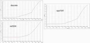
@carlmartSomething is not right. Did you arrange grounds like at attached picture? I’m getting 125 dB PSRR.
C5 and C6 should be connected to the same power ground as load. Remaining circuit ground is Kelvin sense connection ground and only that should be connected to the power ground with small inductance. Check again post #2955.
Simply give smoother phase response in region < 500HzWhat is the reson for using a voltage reference instead of a zener at the opamp output?
Power supply rejection ratio confirms the best on ne5534, load 500mA. This might explain why J.D. regulators improves digital amplifiers sound details expecialy in direct stream digital dacs because of huge PSRR in HF region?
Attachments
Last edited:
OK, now we are on the same tune. -136dB psrr @ 1KHz. OK, I will use these changes on the other opamps.@carlmart
C5 and C6 should be connected to the same power ground as load. Remaining circuit ground is Kelvin sense connection ground and only that should be connected to the power ground with small inductance. Check again post #2955.
Should they be also used for other parameters, like noise or impedance?
What if I do not use the Kelvin links? I don't have space for two separate +/- SR on this preamp. I don't think you can share Kelvin links between two channels.
Yes.Should they be also used for other parameters, like noise or impedance?
Every PCB track has at least a fraction of nH inductance and there are also parasitic capacitances, which make performance of real circuit different from the simulation. This single added inductance helps to get realistic simulation result for low frequency PSRR. Additional parasitic capacitances added with cshunt option, would correct high frequency PSRR. Though, that directive can make simulation hard to run. Plying with additional directives can help, but don’t ask me which ones. It’s tricky.
On the actual PCB, kelvin connections exist. and they are mandatory only to the points of output connector, although they can be extended to the power-in points of circuit supplied by the regulators. Will you design your own PCBs?What if I do not use the Kelvin links? I don't have space for two separate +/- SR on this preamp. I don't think you can share Kelvin links between two channels.
Not at all.Does the opamp not being too low offset a problem with the SR?
Yes, I plan to design my own pcbs. Making the Kelvin traces on the board is easy.Yes.
Every PCB track has at least a fraction of nH inductance and there are also parasitic capacitances, which make performance of real circuit different from the simulation. This single added inductance helps to get realistic simulation result for low frequency PSRR. Additional parasitic capacitances added with cshunt option, would correct high frequency PSRR. Though, that directive can make simulation hard to run. Plying with additional directives can help, but don’t ask me which ones. It’s tricky.
On the actual PCB, kelvin connections exist. and they are mandatory only to the points of output connector, although they can be extended to the power-in points of circuit supplied by the regulators. Will you design your own PCBs?
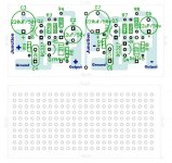
I will build some Denoisators too, but I might try using pre-drilled boards for that. The question is if I go with the slighltly more "tricky" CSC version. Pity it's hard to simulate Denoisator's noise, as the 3X7 don't bring noise model data.
Using a pre-drilled pcb for the SR is more tricky, as there are a lot of parts. The ideal thing would be to so and then send the ones I find best to a pcb factory.
What I do for my prototype PCBs on pre-drilled boards is use any pcb design program for the parts placement and wiring, not improvise them or put parts off the pcb. Everything is pre-designed.
First of all I design a pads matrix, based on several pcb board sizes I already have. Then I use that matrix as the guide to place my parts and traces. For the traces sometimes I use the parts wire (only use TH parts) to reach the following part, and so on and on.
But I am not sure how large should you go using the method.
In this case I designed a piggy-back pcb to attach to a 317/337 regulator.
Attachments
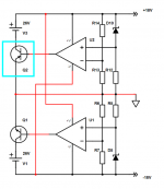
Hello everyone,
I have a somewhat conceptual question. On the attached highly simplified diagram, the regulator on the left is the original Jan Didden's circuit with no changes whatsoever (other than 2 batteries shown). A lot of parts are not shown only to simplify the question. Please imagine they are all still in place. The part numbers are the same as in Jan's circuit.
The regulator on the right is mostly the same, except the positive and negative channels have been flipped. The positive channel is moved from the top to the bottom and produces a negative output voltage. Similarly, the negative channel is moved from the bottom to the top and produces a positive output voltage. Obviously, the original circuit ground is no longer the ground, etc.
The second change is in the power supply of both opamps as shown. This apparently removes the need for the zenners and their filtering capacitors, because the opamps are already properly biased within approximately 0.7V. (The 10-Ohm resistors R3 and R10 between the output of the opamps and the base of the power transistors are still in place, just not shown to simplify the comparison). All changes from the original circuit are highlighted in red.
My question is if the modified circuit would work and if so, does it have any disadvantages compared to the original circuit specifically while using batteries. I realize that batteries are no longer connected to the ground, but I don't see why this would matter for the functionality.
Are there any concerns with noise or anything else? Or is this totally wrong and it would explode with fireworks? I would appreciate any insight. Thank you!
Attachments
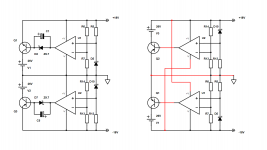
You might encounter extra difficulties in making the right hand circuit stable (i.e. oscillation free). The discrete transistors on the left are operated at voltage gain of ~0.98 volts per volt, while the discrete transistors on the right {see blue box} are operated at voltage gain of at least 50 volts per volt. This extra gain definitely shifts the transfer function of the circuit as a whole, and the new transfer function is likely to be unstable. Requiring additional design effort to provide frequency compensation.
edit- to guarantee that the circuit starts up correctly, instead of stupidly putting out 0V on both rails (because the opamps have no power supply) . . . . I might suggest connecting a 12V zener diode from collector to emitter of the PNP, and a second 12V zener from collector to emitter of the NPN. This ensures that the supply rails will be at least (26 - 12) = 14 volts, which is more than enough to wake up the opamps and let the circuit get started. Then after it all settles, the voltage across the zeners will be only (26 - 18) = 8 volts, and they will not conduct even one microampere of current, so they "disappear". aaaah.
_
Attachments
Last edited:
Thanks Mark, I appreciate it! Here is the part I’m not clear on:
“The discrete transistors on the left are operated at voltage gain of ~0.98 volts per volt, while the discrete transistors on the right {see blue box} are operated at voltage gain of at least 50 volts per volt.”
All relative voltages on all transistors should be the same on the right and left diagrams. Why would the transistors operate differently? Could you please elaborate?
Thanks again,
Alex
Hello friends,
I am building a +5V Super Regulator using Jan's original circuit and board. I understand that the opamp should be biased by about 3.2V to be in the middle of the power supply range. For this purpose, I have the 1N5518 zener (https://www.mouser.com/datasheet/2/268/LDS_0037_1-1592446.pdf) with a low noise of 0.5uV/Hz. Alternatively I can use a couple of 1.7V red LEDs in series in place of D2. Which of these two options is better from the standpoint of noise and performance? My power supply is a 13V battery.
Thanks for your help and expertise!
Alex

So far, we have no intention of making new PCBs for the entire regulator, but only with accessories, i.e. a variable voltage reference and maybe for current sources that will be able to be implemented in every regulator that uses a zener or some other voltage reference such as LM329, LM4040, TL431 etc. for voltage regulation. The announcement will also be here on the forum, so you don't have to worry.This is a fantastic news! Can you please tell us if a circuit board will be available for purchasing? And also the approximate expected timeframe of the announcement (next month, 3 months from now, etc.). Finally, what is the best way to receive this announcement (e.g. an email list or check this thread or check some other website, etc.).
Also thank you for your insight on the best opamps for the Superregulator. What is your opinion on AD797 as opposed to those you have mentioned? And also on OPA828 with the 8V supply (like +/-4V) in a Superregulator with the 13V input and either 8V or 5V output and 0.3A load? Thanks again!
As for the op amps themselves, the OPA1641 is a good choice from 7V and above, there is no need for the expensive OPA828 or AD797. The OPA1641 can be used for voltages lower than 7V, but only with a 1V reference. Below 7V, bipolar op amps are a mandatory choice, such as OPA1611, ADA4897, LT6202, etc.
- Home
- The diyAudio Store
- Super Regulator