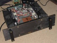
I picked up this amplifier today for next to nothing as it is in need of repair. I really purchased it for the case and power supply and I got it really cheap but when I got it home and had a closer look it seemed like a very well designed piece. Also the damage was more extensive than I imagined.
It is very difficult to find any information on the net about this amplifier but I had a little time and I managed to gather the following and thought to share it.")
It is very difficult to find any information on the net about this amplifier but I had a little time and I managed to gather the following and thought to share it.
Attachments
Break on through...
Originally I thought the VSP Labs amp chassis would make a wonderful home for some new design but I continued to scour the internet to research its origins. I wanted to find out what VSP Labs was all about. It was very difficult as there is very little documentation or information to be had. The opinions I found on the internet boards seem to echo the same information; that the Transmos amplifier was awesome, unique and marketed at too low a sale price.
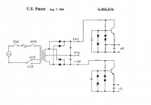
I continued to search the net and then I stumbled upon the VSP “creators” name. Then I Googled this information and I found the patent (earlier posted).
It wasn’t enough for me. I called a bunch of companies that once sold or serviced the VSP products in the US. All I could come up with was a few scanned pages of the owner’s manual. After that I had to drop it for a while but I left the amplifier beside the computer at home and I kept looking at it.
Like some crazed maniac I started to Google the authors name until I found an internet post indicating the firm the author is currently working with. I don’t need to get into the details of all that and it is of no importance or significance to this thread. This thread should remain VSP topic focused.
I called the authors company and left a voice mail in the appropriate mail box. I got a call back the very next day. I am shocked by my actions that I pursued this amp so far and I am amazed at the results. I’m a little embarrassed to share this information but it is now part of the story.
Cheers,
Shawn.
Originally I thought the VSP Labs amp chassis would make a wonderful home for some new design but I continued to scour the internet to research its origins. I wanted to find out what VSP Labs was all about. It was very difficult as there is very little documentation or information to be had. The opinions I found on the internet boards seem to echo the same information; that the Transmos amplifier was awesome, unique and marketed at too low a sale price.
I continued to search the net and then I stumbled upon the VSP “creators” name. Then I Googled this information and I found the patent (earlier posted).
It wasn’t enough for me. I called a bunch of companies that once sold or serviced the VSP products in the US. All I could come up with was a few scanned pages of the owner’s manual. After that I had to drop it for a while but I left the amplifier beside the computer at home and I kept looking at it.
Like some crazed maniac I started to Google the authors name until I found an internet post indicating the firm the author is currently working with. I don’t need to get into the details of all that and it is of no importance or significance to this thread. This thread should remain VSP topic focused.
I called the authors company and left a voice mail in the appropriate mail box. I got a call back the very next day. I am shocked by my actions that I pursued this amp so far and I am amazed at the results. I’m a little embarrassed to share this information but it is now part of the story.
Cheers,
Shawn.
Old School VSP
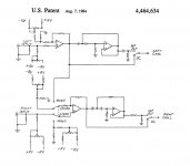
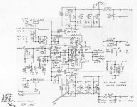
Attached is an earlier copy of the VSP Labs TRANSMOS amplifier schematic and block diagram.
The author has given me permision to share this information but advises this version is not the finished product that VSP produced.
Mr. Velazquez writes,"The hand drawn schematic is useable only for reference or history. It should not be used for building amps as several changes affecting performance and or safety are not in the hand drawn schematic. You may share it on the internet within the context of reference/history with proper credits."
Cheers,
Shawn.
Attachments
Attachments
Production Version
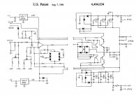
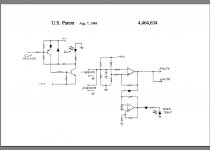
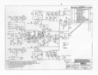
Here is a PDF containing a working production version of the VSP Labs Transmos 150.
Lots more work to do but I see a full restoration coming my way and if I'm lucky there will be tweaks. Any thoughts from the DIY folks here? I'd love to hear your impressions of this circuit!
Cheers,
Shawn.
Here is a PDF containing a working production version of the VSP Labs Transmos 150.
Lots more work to do but I see a full restoration coming my way and if I'm lucky there will be tweaks. Any thoughts from the DIY folks here? I'd love to hear your impressions of this circuit!
Cheers,
Shawn.
Production Version
Here is a PDF containing a working production version of the VSP Labs Transmos 150.
Lots more work to do but I see a full restoration coming my way and if I'm lucky there will be tweaks. Any thoughts from the DIY folks here? I'd love to hear your impressions of this circuit!
Cheers,
Shawn.
Here is a PDF containing a working production version of the VSP Labs Transmos 150.
Lots more work to do but I see a full restoration coming my way and if I'm lucky there will be tweaks. Any thoughts from the DIY folks here? I'd love to hear your impressions of this circuit!
Cheers,
Shawn.
Great stuff - I just got one of these on ebay pretty much on a whim - thought at least it would be a good source of parts. Hooked it up and was impressed with sound but found after a while one side got warm (don't think those big heat sinks could ever get hot) and distorted. One by one I removed the 10 amp fuses and replaced them with a multimeter to measure current and found:
left + 270 mA
left - 390 mA and quickly increased off scale
right + 90 mA
right - 270 mA
(if these sound totally wack, maybe I should do this without the vodka)
Do you have any idea what they should be?
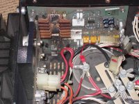
I thought about disconnecting the 100/150 ohm gate resisters leaving just one connected at a time and determining if one or more of the outputs in each section is drawing an abnormal amount of current. Is something bad going to happen to an output device if I leave its gate floating or should I ground them?
If I have to replace an output I don't think I will be able to match the others - I guess you noticed they all have their gain or whatever written on them. So am I better off just putting in a mismatched device or add source resistors to all of them?
left + 270 mA
left - 390 mA and quickly increased off scale
right + 90 mA
right - 270 mA
(if these sound totally wack, maybe I should do this without the vodka)
Do you have any idea what they should be?
I thought about disconnecting the 100/150 ohm gate resisters leaving just one connected at a time and determining if one or more of the outputs in each section is drawing an abnormal amount of current. Is something bad going to happen to an output device if I leave its gate floating or should I ground them?
If I have to replace an output I don't think I will be able to match the others - I guess you noticed they all have their gain or whatever written on them. So am I better off just putting in a mismatched device or add source resistors to all of them?
jbol said:Great stuff ...
Do you have any idea what they should be?
Send me some Vodka and then we'll both understand each other better.
Just kidding. I have not fully embraced this project yet as I have been debating to etch an entire new set of PCBs for my amp or try very hard to clone the original driver board. After I move I'll get set up again and then I'll get my strategy together.Meanwhile I will contact the author and see if he will drop in and lend a hand.
Hang on...
Shawn.
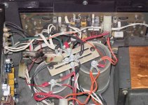
Pre and driver in tough times.
It looks like the voltage regulators get too hot - my board looks a little toasty in that area but not cooked like yours (I think it works fine but I am going to give it a closer look) - is there any info that I get get from mine that might be useful to you?
jim
It looks like the voltage regulators get too hot - my board looks a little toasty in that area but not cooked like yours (I think it works fine but I am going to give it a closer look) - is there any info that I get get from mine that might be useful to you?
jim
Re: Pre and driver in tough times.
If you have one working channel, the schematic printed out, then there is nothing stopping you from fixing it, assuming you are good at electronic trouble shooting. Simply measure the good channel and compare to the bad channel and then look at the schematic. What is the DC offset?
Can ya dig it? There is sooooooo much you can check if you have a working channel.
As jdk has suggested there are obsolete parts. I think the outputs were matched sets as well. Have you disconnected the wire harness system for voltage readings?
Jim you have a lot of work to do & you have the schematics. Back to the bench and don't blow up the working channel when you are tinkering around in there.
Shawn.
jbol said:It looks like the voltage regulators get too hot - my board looks a little toasty in that area but not cooked like yours (I think it works fine but I am going to give it a closer look) - is there any info that I get get from mine that might be useful to you?
jim
If you have one working channel, the schematic printed out, then there is nothing stopping you from fixing it, assuming you are good at electronic trouble shooting. Simply measure the good channel and compare to the bad channel and then look at the schematic. What is the DC offset?
Can ya dig it? There is sooooooo much you can check if you have a working channel.
As jdk has suggested there are obsolete parts. I think the outputs were matched sets as well. Have you disconnected the wire harness system for voltage readings?
Jim you have a lot of work to do & you have the schematics. Back to the bench and don't blow up the working channel when you are tinkering around in there.
Shawn.
Am I wrong in assuming that the N channels should be running at the same bias as the P channels? It could be that one side just has a couple of open circuit outputs on one half (270 mA versus 90 mA - 3 to 1). The side that gets hot worries me more since the bias seems to take off on one half. I will get a better chance to check it out soon - our house is getting painted inside so I am living down the road.
"Originally posted by jbol
It looks like the voltage regulators get too hot - my board looks a little toasty in that area but not cooked like yours (I think it works fine but I am going to give it a closer look) - is there any info that I get get from mine that might be useful to you?"
what I meant was anything useful to you in fixing yours.
- Status
- This old topic is closed. If you want to reopen this topic, contact a moderator using the "Report Post" button.
- Home
- Amplifiers
- Solid State
- VSP LABS Trans Mos Amplifier