I'm not being totally facetious when I suggest using some kind of clipping/overload detector/indicator, and advise one and all to just NOT CLIP THE AMP! I used to just connect a scope across the output terminals, which was quite instructive and caused no sonic ill effects. Much of the discussion I see around amplifier design is about having amps with sufficient clean power output to *never* have clipping. It's obnoxious, it's dangerous, and most of all, it's not good for your ears.
Now if you are folks who are not listening at home and are doing monitoring in studios, etc, and the head-bangers who want to hear what it sounds like when it's really loud are paying the bills, then some form of unobtrusive hearing protection is a really good idea. Having been there, I recommend it highly.
However, if you;re listening at home, perhaps your solution will be to use speakers with decently higher voltage sensitivity/efficiency, so that your megawatt monsters just don't ever have to work that hard.
Really. End of rant.
Hi Richiem,
You're right, its best if amps don't clip - and many don't realise how often they clip when playing music at realistic levels, especially if the speaker efficiency is only modest. Mitigation of clipping effects is important, like the use of Baker clamps. A soft clip circuit in front of the amplifier that adapts to available rail voltage is also very effective, since it prevents the amplifier-proper from ever clipping.
Cheers,
Bob
Mystifying TMC, correction
Regarding a previous post of mine, I have to confess that I made an stupid error. Due to a wrong sign (+ instead of -) the reported currents are NOT correct. My sincere apologies for this embarrassing blunder.
Here are the new data, which I believe are correct.
This time, I also have simmed the IPS output current (Io) under slightly different conditions: first with a sine wave of 20kHz (instead of 100kHz) and 1Vpk, next with a square wave with the same frequency and amplitude. Also the VAS output current (Iv) is given, peak values.
Sine wave:
CMC: Io = 168uA; Iv = 183uA
TPC: Io = 8uA; Iv = 1.77mA
TMC: Io = 179uA; Iv = 74uA
Indeed, as stated by Ophelia, the IPS has to deliver the highest current in case of TMC, though compared to conventional Miller compensation (CMC) the difference is negligible. Regarding the VAS output current however, the picture is totally different: the highest for TPC.
But we are still not done. As it is common practice to torture amps with a square wave, let's look at the currents under this condition:
Square wave:
CMC: Io = 4.37mA; Iv = 4.76mA
TPC: Io = 4.76mA; Iv = 47.9mA
TMC: Io = 4.35mA; Iv = 4.53mA
As can be seen, now IPS and VAS currents are lowest in case of TMC. So, Ophelia's conclusion that:
> On the flip side, TMC extra loads the input stage, with the equivalent lead-lag compensation network Miller reflection. For identical global amp
> results, this may require a beefier input stage (more current, more degeneration, etc...) compared to simple Miller or TPC compensation.
still doesn't hold water.
Cheers,
E.
PS: Compensation component values: C1 = 68pF C2 = 680pF, R1 = 330R
The square wave has been 'conditioned' by means of a LP input filter (330R, 1nF) in order to limit the SR to a modest 54V/us.
PS: Compensation component values: C1 = 68pF C2 = 680pF, R1 = 330R
Don't forget you can swap C1 and C2 in the case of TPC to give significantly lower Iv numbers should you so desire. Unity Loop Gain frequency, the zero frequency and phase margin remain the same.
C1 > C2 instead of C1 < C2
Hi Harry,
Good point! Indeed, figures are much better now. When subjected to a (filtered) square wave, I got Io = 4.04mA and Iv = 6.64mA (instead of a crazy 47.9mA).
Thanks for your hint.
Cheers,
E.
Don't forget you can swap C1 and C2 in the case of TPC to give significantly lower Iv numbers should you so desire. Unity Loop Gain frequency, the zero frequency and phase margin remain the same.
Hi Harry,
Good point! Indeed, figures are much better now. When subjected to a (filtered) square wave, I got Io = 4.04mA and Iv = 6.64mA (instead of a crazy 47.9mA).
Thanks for your hint.
Cheers,
E.
Unfortunately, doing that loads the input of the VAS heavily, reducing it's open-loop gain. The final result is likely to be much higher distortion.Don't forget you can swap C1 and C2 in the case of TPC to give significantly lower Iv numbers should you so desire. Unity Loop Gain frequency, the zero frequency and phase margin remain the same.
Some sort of compromise might be best e.g. C1 = C2 = 120pF, R1 = 1K.
The idea is that it may be better to worsen two different aspects of performance by a factor of 2, rather than worsening one by a factor of 10 in order to achieve minimal degradation of the other.
I just ran a simulation on a balanced VAS amp and put it into clipping. Result:- No collapse of the VAS standing current (I run at 30mA).
Another good reason for balanced drive topologies in my book.
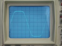
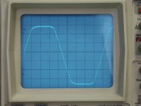
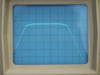
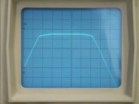
Another plus to the fully comp. is the almost "soft clipping" characteristic it exhibits (at least on my soon to be actually completed CLX - below 1)
I can't wait to actually clip this voltage stage on my 40V rail OPS to see whether LT "lies" ...
Hi Richiem,
You're right, its best if amps don't clip - and many don't realise how often they clip when playing music at realistic levels, especially if the speaker efficiency is only modest. Mitigation of clipping effects is important, like the use of Baker clamps. A soft clip circuit in front of the amplifier that adapts to available rail voltage is also very effective, since it prevents the amplifier-proper from ever clipping.
Cheers,
Bob
But the end user is not always prudent , so higher than needed rails in addition to "crippled" gain ( less than would be needed to create clipping at 2V inputs). I have a input switch on the rear of the amp to halve the input signal , keeps the kids from blowing woofers with their dang movies...
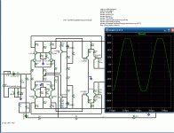
With the amp below , I would not be as concerned except for the obscene amount of power you would actually be AT with 140V p-p !! OS
Attachments
Unfortunately, doing that loads the input of the VAS heavily, reducing its open-loop gain. The final result is likely to be much higher distortion.
This is not correct. The order of C1 and C2 have no effect on the loop gain of the amplifier (both circuit analysis and simulation verify this).
Last edited:
Unfortunately, doing that loads the input of the VAS heavily, reducing it's open-loop gain. The final result is likely to be much higher distortion.
Some sort of compromise might be best e.g. C1 = C2 = 120pF, R1 = 1K.
The idea is that it may be better to worsen two different aspects of performance by a factor of 2, rather than worsening one by a factor of 10 in order to achieve minimal degradation of the other.
Hi Godfrey,
This is a good example where some simulation of distortion of an actual amplifier design might be very helpful.
In some designs the size of these capacitors may be quite small, as well, depending on the amount of degeneration and tail current in the IPS (for a given gain crossover frequency). Also, a VAS stage with a healthy standing current may be less susceptible to such loading causing distortion. Finally, this sort of issue probably makes a good case for a push-pull VAS (i.e., not a blameless-like design).
Cheers,
Bob
Unfortunately, doing that loads the input of the VAS heavily, reducing it's open-loop gain. The final result is likely to be much higher distortion.
Some sort of compromise might be best e.g. C1 = C2 = 120pF, R1 = 1K.
The idea is that it may be better to worsen two different aspects of performance by a factor of 2, rather than worsening one by a factor of 10 in order to achieve minimal degradation of the other.
Hi Godfrey,
In principle, I agree with the idea of 'balancing' the evil (capacitive) loading effects on the IPS output and VAS output. However, the VAS input voltage is much, much smaller than the VAS output voltage. This means that the loading effect of C1 (i.e the current through C1) is also much smaller that C2. For this reason, taking C1 >> C2 does not degrade the performance.
As a matter of fact, the IPS output current (Io) is even smaller if C1>>C2.
In the simulations as used in post #3306 and 3308, C1=68pF & C2=680pF, respectively C1=680pF & C2=68pF. In the first case, Io=8uA and in the latter case Io=6uA (at Vi=1V and 20kHz).
Cheers,
E.
Quite right, my bad.This is not correct. The order of C1 and C2 have no effect on the loop gain of the amplifier (both circuit analysis and simulation verify this).
I did some sims as Bob suggested and found that swapping the caps makes negligible difference to either the bode plots or distortion with any kind of sensible load (e.g. 100K+) on the VAS output. The kind of degradation I was expecting only shows up with very heavy loads e.g. 1 to 10K.
My concern was to do with the current gain of the VAS. An "ideal" VAS would have a low input impedance, and act as a virtual earth input device. However, a Blameless-style Darlington VAS has a very high input impedance (and, potentially, a very high current gain).However, the VAS input voltage is much, much smaller than the VAS output voltage. This means that the loading effect of C1 (i.e the current through C1) is also much smaller that C2. For this reason, taking C1 >> C2 does not degrade the performance.
If we consider the VAS with local feedback via C2 initially disconnected, it's current gain at highish frequencies is limited approximately to the impedance of C1 divided by it's effective emitter resistance. So increasing C1 reduces the VAS's current gain.
I expected that when local feedback is then applied, the reduced current gain would result in increased output impedance, and thus worse results driving a nonlinear load. Apparently not.
Perhaps it would be more correct to think of the VAS as a voltage operated device at high frequencies. I suppose that makes sense since whichever value cap is used for C!, it's impedance is likely to be lower than the VAS's inherent input impedance.
Back to the sims....
Cheers - Godfrey
Member
Joined 2009
Paid Member
Another plus to the fully comp. is the almost "soft clipping" characteristic it exhibits (at least on my soon to be actually completed CLX - below 1)
Are you saying that you can get soft clipping automatically by implementing TMC?
the VAS is a current to voltage amplifier.An "ideal" VAS would have a low input impedance, and act as a virtual earth input device. However, a Blameless-style Darlington VAS has a very high input impedance (and, potentially, a very high current gain).........................
Perhaps it would be more correct to think of the VAS as a voltage operated device at high frequencies. I suppose that makes sense since whichever value cap is used for C!, it's impedance is likely to be lower than the VAS's inherent input impedance.
It uses the current in the collector resistor and converts that to a voltage.
Would that make the input impedance equal to the value of the collector resistor?
Certainly the LTP sees that collector resistor as it's load, making the collector resistor the load impedance. Surely what is load impedance seen from the LTP viewpoint becomes the input impedance seen from the VAS viewpoint.
Are you saying that you can get soft clipping automatically by implementing TMC?
That is not a TMC amp. It's "soft clipping" characteristics are the result of the topology itself.
TMC seems not to behave too well during clipping , that is why I reduced the {Rtmc= 820/1k} on my AX amp. Perfect compromise.
OS
Member
Joined 2009
Paid Member
the VAS is a current to voltage amplifier.
It uses the current in the collector resistor and converts that to a voltage.
Would that make the input impedance equal to the value of the collector resistor?
Certainly the LTP sees that collector resistor as it's load, making the collector resistor the load impedance. Surely what is load impedance seen from the LTP viewpoint becomes the input impedance seen from the VAS viewpoint.
I always view transistors as voltage controlled current devices. I view the load on the LTP is the impedance looking into the base of the VAS device in parallel with the resistor from that base to the -Ve rail. Maybe this is wrong.
The a.c. impedance into the base of a BJT in common emitter configuration depends heavily on the miller capacitance, in this case dominated by Cdom and the load on the output of the collector reflected back to the base by what is confusingly called the current gain.
I think the LTP sees mostly Cdom.
the VAS is a current to voltage amplifier.
It uses the current in the collector resistor and converts that to a voltage.
Would that make the input impedance equal to the value of the collector resistor?
Certainly the LTP sees that collector resistor as it's load, making the collector resistor the load impedance. Surely what is load impedance seen from the LTP viewpoint becomes the input impedance seen from the VAS viewpoint.
The VAS can be looked at in a number of different ways, especially depending on whether one includes the shunt feedback provided by the Miller capacitor or other compensation. At frequencies above the open loop 3 dB bandwidth, the VAS acts like a transimpedance amplifier, essentially with a low-impedance input, like a virtual ground, created by the shunt feedback. It is thus a current-in, voltage-out device over most of its working bandwidth.
At least, this is the way that I look at it.
I always note that some people view a BJT as a chunk of current gain, while others prefer to view it as a chunk of transconductance. Both views lead to the same correct result if analyzed properly. Sometimes what is the best view depends on the type of circuit the device is in.
Cheers,
Bob
- Home
- Amplifiers
- Solid State
- Bob Cordell Interview: Negative Feedback