Hi there,
I have been working on my amplifier at the weekend and I ran into some
confusion according the voltage gain and biasing stage.
One might ask the question why I spend my time to figure out such things
(voltage gain stages), lot of such topology is already available on the
Internet...Well, the truth is, that my mind was concerning too much about
topologies just to build someone's idea. If it is possible I want to build
an amplifier which at least in part a bit mine...And of course I have my
reasons why I tried to make things like in the topology below.
- I do not like symmetrical designs, because 1) "n" and "p" channel devices
are never completely complementary to each other, we all know this, 2) I
would like to use JFETs beacuse of their tube like caracteristic and finding
complementary JFETs are even more trouble, at least for me. So assymmetrical
design is one point.
- I tried to avoid differential amplifier at the input, beacuse the concjept
of it is based on the similarity of the involved parts. Some special BJTs
(MAT02 e.g) can provide a good result, but again I can not mach JFETs so
easily. (Of course there is something like the MAT02 with JFETs, but it is
very expensive. Check it at Borbely's site...). So, avoiding differential
amplifier was the second criteria.
- I like to use grounded base topology beacuse the gate or base capacitance is
no more a limiting factor when driving the stage. It means fast operation
with wide frequency range providing enough margin to the negative feedback
and higher slew rate can be achieved in this way with the same amount of
driving current which equals to lower dynamic intermodulation torsition.
(Source: Mark Alexander - A current Feedback Power Amplifier.) So grounded
emitter topology is not welcommed.
- DC connection at the input and at the output as well. This may not needs
further explanations why.
- Next criteria is to use as less stage in the voltage amplifying process as
possible. In this case it means two. It is beacuse I decided to use the CEF
as the output stage - I explain it later why. I could not figure out any one
stage topology which provides at least 15 gain having its input at zero volt
and its output near to 1 Volts. (Of course the output of a bridged amplifier
can be anything providing that both output has the same amount of DC. But
again, building completly similar amplifiers is a question of part matching
which I want to avoid. Even with X-feeback it is recommended to select the
MOSFETs as far as I know...) So, a to stage topology is likely what we can
have.
And why I used CEF, which uses BJTs insted of MOSFETs (of course the second
BJT in the CEF can be a MOSFET, but do I have to pair them?), it is even
symmetrical, and the second BJT works as a grounded emitter? The short
answer is beacuse it can be operated in free "run", which means that I do
not have to inculde it in the global feedback. It provides low output
impedance and fairlry low distorsion. It is something I like and want to
use. Besides, with a multimeter I can easily pair BJTs according to their
hfe and as far as I know BJTs are much more complemetary to each other as
the MOSFETs. And one more point, which is maybe a bit controversial...I
think the CEF is the only type of output stage which can benefit from the
theory of the split feedback. I do not describe here what "split feedback"
means, anyone who is unfamiliar with it can easily find out what it means
with the help of the search button above...The topology below does not
include it, but it is easy to imagine how it fits there. The CEF stage
already there moves into the loop and an another one gets in paralell
staying out of the feedback. The last reason to use a symmetrical output is
thus in this way the output current is not limited in a way as in the SE
outputs.
(Warning for newbies! (including me) The information above is not qualified
to be truth, before beliving what I have just typed wait for the reactions.
I may wrong in some or every statment I made here.)
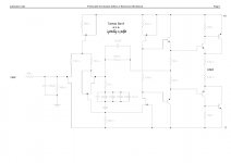
So, that is the background of this topology. Sorry for being long, but I wanted to avoid questions about why I tried to do it in this way.
And now heading for my problem: Is this working??? I simulated it with
Electronics Workbench and sometimes it manages to calculate everything, (and
then it seems to be a HiFi power amplifer) sometimes the transient behavior
and the Fourie is an impossible task for it. Strange. Even more strange that
the THD does not changes at the output wheter I inculde the CEF in the
feedback or not, wheter I connect a 4 Ohms load or not. First I thought,
that the topology is may be instable, but the fact that sometimes it can be
simulated is against that. I tried to simulate a Borbely like symmetrical
cascoded two stage differential amplifier based (you know...) voltage gain
and the program was unable to calculate it. (I have backengineered the
values of some topologies available on Borbely's site and I've even modified
one which was staded as a working concept regarding Mr. Borbely (We had a
mail change about it some years ago) and using my schools simulator it was
stable. Here, it does not worked at all.)
So before buying all the parts and designing a PCB for it I call all the
experts to help me about getting sure about this topology...(And hey, I
could simulate it as many times as I coudn't, so hope is dying last...)
Oh, I almost forgot. The cascoding is used beacuse the feedback signal
drives the JFET as a gronded emitter and I wanted to speed up things.
Besides, the simulator does not showed any interested in it. Nothing has
changed with cascoding that stage....
And at least, this is just a first draw, for example the DC offset is to solve here. (Maybe with a comparator/integrator conncected to the second current source)
Anyway, thanks reading this...
bt
I have been working on my amplifier at the weekend and I ran into some
confusion according the voltage gain and biasing stage.
One might ask the question why I spend my time to figure out such things
(voltage gain stages), lot of such topology is already available on the
Internet...Well, the truth is, that my mind was concerning too much about
topologies just to build someone's idea. If it is possible I want to build
an amplifier which at least in part a bit mine...And of course I have my
reasons why I tried to make things like in the topology below.
- I do not like symmetrical designs, because 1) "n" and "p" channel devices
are never completely complementary to each other, we all know this, 2) I
would like to use JFETs beacuse of their tube like caracteristic and finding
complementary JFETs are even more trouble, at least for me. So assymmetrical
design is one point.
- I tried to avoid differential amplifier at the input, beacuse the concjept
of it is based on the similarity of the involved parts. Some special BJTs
(MAT02 e.g) can provide a good result, but again I can not mach JFETs so
easily. (Of course there is something like the MAT02 with JFETs, but it is
very expensive. Check it at Borbely's site...). So, avoiding differential
amplifier was the second criteria.
- I like to use grounded base topology beacuse the gate or base capacitance is
no more a limiting factor when driving the stage. It means fast operation
with wide frequency range providing enough margin to the negative feedback
and higher slew rate can be achieved in this way with the same amount of
driving current which equals to lower dynamic intermodulation torsition.
(Source: Mark Alexander - A current Feedback Power Amplifier.) So grounded
emitter topology is not welcommed.
- DC connection at the input and at the output as well. This may not needs
further explanations why.
- Next criteria is to use as less stage in the voltage amplifying process as
possible. In this case it means two. It is beacuse I decided to use the CEF
as the output stage - I explain it later why. I could not figure out any one
stage topology which provides at least 15 gain having its input at zero volt
and its output near to 1 Volts. (Of course the output of a bridged amplifier
can be anything providing that both output has the same amount of DC. But
again, building completly similar amplifiers is a question of part matching
which I want to avoid. Even with X-feeback it is recommended to select the
MOSFETs as far as I know...) So, a to stage topology is likely what we can
have.
And why I used CEF, which uses BJTs insted of MOSFETs (of course the second
BJT in the CEF can be a MOSFET, but do I have to pair them?), it is even
symmetrical, and the second BJT works as a grounded emitter? The short
answer is beacuse it can be operated in free "run", which means that I do
not have to inculde it in the global feedback. It provides low output
impedance and fairlry low distorsion. It is something I like and want to
use. Besides, with a multimeter I can easily pair BJTs according to their
hfe and as far as I know BJTs are much more complemetary to each other as
the MOSFETs. And one more point, which is maybe a bit controversial...I
think the CEF is the only type of output stage which can benefit from the
theory of the split feedback. I do not describe here what "split feedback"
means, anyone who is unfamiliar with it can easily find out what it means
with the help of the search button above...The topology below does not
include it, but it is easy to imagine how it fits there. The CEF stage
already there moves into the loop and an another one gets in paralell
staying out of the feedback. The last reason to use a symmetrical output is
thus in this way the output current is not limited in a way as in the SE
outputs.
(Warning for newbies! (including me) The information above is not qualified
to be truth, before beliving what I have just typed wait for the reactions.
I may wrong in some or every statment I made here.)
So, that is the background of this topology. Sorry for being long, but I wanted to avoid questions about why I tried to do it in this way.
And now heading for my problem: Is this working??? I simulated it with
Electronics Workbench and sometimes it manages to calculate everything, (and
then it seems to be a HiFi power amplifer) sometimes the transient behavior
and the Fourie is an impossible task for it. Strange. Even more strange that
the THD does not changes at the output wheter I inculde the CEF in the
feedback or not, wheter I connect a 4 Ohms load or not. First I thought,
that the topology is may be instable, but the fact that sometimes it can be
simulated is against that. I tried to simulate a Borbely like symmetrical
cascoded two stage differential amplifier based (you know...) voltage gain
and the program was unable to calculate it. (I have backengineered the
values of some topologies available on Borbely's site and I've even modified
one which was staded as a working concept regarding Mr. Borbely (We had a
mail change about it some years ago) and using my schools simulator it was
stable. Here, it does not worked at all.)
So before buying all the parts and designing a PCB for it I call all the
experts to help me about getting sure about this topology...(And hey, I
could simulate it as many times as I coudn't, so hope is dying last...)
Oh, I almost forgot. The cascoding is used beacuse the feedback signal
drives the JFET as a gronded emitter and I wanted to speed up things.
Besides, the simulator does not showed any interested in it. Nothing has
changed with cascoding that stage....
And at least, this is just a first draw, for example the DC offset is to solve here. (Maybe with a comparator/integrator conncected to the second current source)
Anyway, thanks reading this...
bt
Attachments
Thanks Banfi T. for sharing your idea.
Thanks Banfi T. for sharing your idea.
I have taken a copy into my documents.
I call it: banfi_amp_01.jpg - as this is version 1
Will study it.
I am sure you will get suggestions
on parts and eventual changes.
/halojoy - likes new ideas
Thanks Banfi T. for sharing your idea.
I have taken a copy into my documents.
I call it: banfi_amp_01.jpg - as this is version 1
Will study it.
I am sure you will get suggestions
on parts and eventual changes.
/halojoy - likes new ideas
Sorry for spelling mistakes I made...
Between I decided that I try to get somehow an another simulator because I got errors simulating a simple differential amplifier (no current source, some emitter and collector resistance, the simpliest you could imagine...). Nonsense. To my greatest regret I can not progress with the design without a working simulator. Maybe the DC reference problem...
I am reporting back when I have something new to say, anyway, I am still waiting for comments...
Halojoy...tell me that you named it after me because you haven't seen this shematic yet!

(Which is of course not a great deal if it does not work...)
Ups! I haven't noticed yet that the value of the supply voltage is missing...It is +/- 20 Volts regulated, but of course it can be greater or less as well....
Between I decided that I try to get somehow an another simulator because I got errors simulating a simple differential amplifier (no current source, some emitter and collector resistance, the simpliest you could imagine...). Nonsense. To my greatest regret I can not progress with the design without a working simulator. Maybe the DC reference problem...
I am reporting back when I have something new to say, anyway, I am still waiting for comments...
Halojoy...tell me that you named it after me because you haven't seen this shematic yet!
(Which is of course not a great deal if it does not work...)
Ups! I haven't noticed yet that the value of the supply voltage is missing...It is +/- 20 Volts regulated, but of course it can be greater or less as well....
Yes, voltage supply
That is a most forgotten thing
in amplifier schematics -
At what voltage, is the amplifier going to work.
I always use a specific Volt Value,
when I try to design an amplifier.
Sorry to say, on the web, That important Data is missing.
Even if an amplifier can work well over a wide area of voltages,
there is one Recommended, and Limits (highest, lowest)
This is given in the datasheets of Power Amp Chips.
But not by those so kinda "amp experts"
on their websites.
At least it is missing too many timnes!
halojoy knows - he has been around the www for awhile
Thanks for the question halojoy...
To be honest - and to my greatest regret - this project is sleeping now. The simulator I have is nothing but a big sh*t, I know this for now...Meantime I tried to get some JFET here locally and you wouldn't believe, but only one type of JFET is available here! No p-channel device!!
I wanted to build just the voltage gain stage in the lab of my formerly school to see how it performs, but without the parts it is very hard indeed...
However I still think, that it would work and have a very unique "voice". Besides I wonder about that no one had any comment about it. I know that a lot of smart and experinced people are around here every day...(including the One and Only)
But I'm not giving up my hobby of course. I have ordered today the parts of my next power amplifier. It is fully BJT based and voltage gain stages are cascoded. At the input I am using a MAT04 quad BJT. It will have an exotic look because cascode stage biasing is done via blue LEDs. (They have about 3.7 voltage drop...)
I am working on the chassis in this weekend and I am expecting to finish it within a month or so...I will post the topology and pictures then to a new topic.
cheers:
bt
Banfi T. said:Thanks for the question halojoy...
The simulator I have is nothing but a big sh*t, I know this for now...Meantime I tried to get some JFET here locally and you wouldn't believe, but only one type of JFET is available here!
No p-channel device!!
I have ordered today the parts of my next power amplifier. It is fully BJT based and voltage gain stages are cascoded. At the input I am using a MAT04 quad BJT. It will have an exotic look because cascode stage biasing is done via blue LEDs. (They have about 3.7 voltage drop...)
cheers:
bt
I do not SIMULATE - reasons are many
but in short It is not reality - when it comes to parts
It is hard enough to find true Complementart Bipolars
JFETs - never!
If my Wth was higher (high Wth* have N.Pass & P.Daniel and some few others at www.diyaudio.com )
 I would buy some MAT-0X devices. It is the best input stage you can select - IN WHOLE WORLD!!
 Consider 2 Red LEDS in series instead.
My research, as well as other on forum,
indicates that this gives best, most constant
output from Currents Source. When used with bipolar.
It should be in close cotact. Have almost same temp koefficient.
Green and other diodes 1N4148 did not work as well.
I wouldn't imagine BLUE either.
Use RED LEDs.
Only alternative would be same bipolar BC550C
used as an amplified diode.
You can select any voltage, with help of variable resistor,
and temp coefficient would be same.
JFETS are good as current source
for the LED (the voltage ref) in the bipolar Current Source.
That is MY BEST use of JFETs Each thing in its best place!
/halo - gives you a Tangband Pic - just as a bonus!
------------------------------------------------------
** Wth
a concept invented by halojoy, where he say you can judge
the designers Wth, by examine theor constructions.
Wth is a limiting factor in designs, for most of peoples on this earth
It even makes different dinner tables look slightly
different, all around this world; Bangladesh or Guatemala ...
-----------
Wth stands for Wallet-THickness
and was first mentioned in "Heat Issues" thread in PASS forum.
Noone dared to post an answer - especially not Nelson, the Forum owner
Well, some poor people lack courage Attachments
Hi there, thanks for the inputs...
PCP, how about single ended topology?
halojoy,
"I do not SIMULATE - reasons are many
but in short It is not reality - when it comes to parts."
I agree. But IMHO a simulator is a good tool (if it works) just one has to know how to use it. I mean, design ideas for any audio amplifier should not come from trying things on the simulator or experiencing things through the simulator. One would end up designing a discrete version of some op amp with too much NFB... I have been through this... But on the other side I have designed a lot of amplifer which does not worked at all or had very high distorsion. Just beacuse I was unaware of something or because I did not know something. It happens all the time. As someone said here in the forum: Do you know about any amplifier which does not work on simulator but works in real circumstances?
"Consider 2 Red LEDS in series instead.
My research, as well as other on forum,
indicates that this gives best, most constant
output from Currents Source."
For the current source I do use red leds. Blues are for the cascode reference...
And last but not least thank you for the link Werner - already downloaded, will see how it goes.
bt
You know what I mean
You amp is not single ended, either...
Even single ended can be undestood that way. Make a cass- A Sziklay output stage (similar as yours), and put a big electrolite cap ascross the 100 ohm resistor. You've got a current source instead.. and this way it's a single ended.
I've always liked this emoticon
Some useful models:
.model J2sj74 PJF(Beta=92.12m Rs=7.748 Rd=7.748 Betatce=-.5 Lambda=4.464m
+ Vto=-.5428 Vtotc=-2.5m Cgd=85.67p M=.3246 Pb=.3905 Fc=.5
+ Cgs=78.27p Isr=129.8p Nr=2 Is=12.98p N=1 Xti=3 Alpha=10u Vk=100
+ Kf=26.64E-18 Af=1)
.model J2sk147 NJF(Beta=83.15m Rs=1.055 Rd=1.055 Betatce=-.5 Lambda=824.7u
+ Vto=-.3535 Vtotc=-2.5m Cgd=46.24p M=.3582 Pb=.3905 Fc=.5
+ Cgs=70.25p Isr=84.77p Nr=2 Is=8.477p N=1 Xti=3 Alpha=10u Vk=100
+ Kf=29.26f Af=1)
.model J2sk170 NJF(Beta=59.86m Rs=4.151 Rd=4.151 Betatce=-.5 Lambda=1.923m
+ Vto=-.5024 Vtotc=-2.5m Cgd=20p M=.3805 Pb=.4746 Fc=.5
+ Cgs=25.48p Isr=84.77p Nr=2 Is=8.477p N=1 Xti=3 Alpha=10u Vk=100
+ Kf=111.3E-18 Af=1)
.model J2sk389 NJF(Beta=51.76m Rs=8.008 Rd=8.008 Betatce=-.5 Lambda=11.22m
+ Vto=-.5275 Vtotc=-2.5m Cgd=18.28p M=.3367 Pb=.3905 Fc=.5
+ Cgs=20.07p Isr=112.8p Nr=2 Is=11.28p N=1 Xti=3 Alpha=10u Vk=100
+ Kf=92.85E-18 Af=1)
.model J2sk369 NJF(Beta=82.61m Rs=1.556 Rd=1.556 Betatce=-.5 Lambda=414.5u
+ Vto=-.3552 Vtotc=-2.5m Cgd=46.72p M=.3623 Pb=.3905 Fc=.5
+ Cgs=70.51p Isr=86.47p Nr=2 Is=8.647p N=1 Xti=3 Alpha=10u Vk=100
+ Kf=74.85E-18 Af=1)
.model BC546A NPN(Is=7.049f Xti=3 Eg=1.11 Vaf=127.9 Bf=253 Ise=96.26f
+ Ne=1.556 Ikf=77.05m Nk=.5305 Xtb=1.5 Br=1 Isc=130.8f Nc=1.602
+ Ikr=3.321 Rc=.8766 Cjc=5.25p Mjc=.3147 Vjc=.5697 Fc=.5
+ Cje=11.5p Mje=.6715 Vje=.5 Tr=10n Tf=409.5p Itf=1.994 Xtf=40.12
+ Vtf=10)
* PHILIPS pid=bc546a case=TO92
* 91-07-31 dsq
*$
.model BC546B NPN(Is=7.049f Xti=3 Eg=1.11 Vaf=62.79 Bf=374.6 Ise=68f Ne=1.576
+ Ikf=81.57m Nk=.4767 Xtb=1.5 Br=1 Isc=12.4f Nc=1.835 Ikr=3.924
+ Rc=.9747 Cjc=5.25p Mjc=.3147 Vjc=.5697 Fc=.5 Cje=11.5p
+ Mje=.6715 Vje=.5 Tr=10n Tf=410.2p Itf=1.491 Xtf=40.06 Vtf=10)
* PHILIPS pid=bc546b case=TO92
* 91-07-31 dsq
*$
.model BC547A NPN(Is=7.049f Xti=3 Eg=1.11 Vaf=127.9 Bf=253 Ise=96.26f
+ Ne=1.556 Ikf=77.05m Nk=.5305 Xtb=1.5 Br=1 Isc=130.8f Nc=1.602
+ Ikr=3.321 Rc=.8766 Cjc=5.25p Mjc=.3147 Vjc=.5697 Fc=.5
+ Cje=11.5p Mje=.6715 Vje=.5 Tr=10n Tf=409.5p Itf=1.994 Xtf=40.12
+ Vtf=10)
* PHILIPS pid=bc546a case=TO92
* 91-07-31 dsq
*$
.model BC547B NPN(Is=7.049f Xti=3 Eg=1.11 Vaf=62.79 Bf=374.6 Ise=68f Ne=1.576
+ Ikf=81.57m Nk=.4767 Xtb=1.5 Br=1 Isc=12.4f Nc=1.835 Ikr=3.924
+ Rc=.9747 Cjc=5.25p Mjc=.3147 Vjc=.5697 Fc=.5 Cje=11.5p
+ Mje=.6715 Vje=.5 Tr=10n Tf=410.2p Itf=1.491 Xtf=40.06 Vtf=10)
* PHILIPS pid=bc546b case=TO92
* 91-07-31 dsq
*$
.model BC548B NPN(Is=7.049f Xti=3 Eg=1.11 Vaf=62.79 Bf=374.6 Ise=68f Ne=1.576
+ Ikf=81.57m Nk=.4767 Xtb=1.5 Br=1 Isc=12.4f Nc=1.835 Ikr=3.924
+ Rc=.9747 Cjc=5.25p Mjc=.3147 Vjc=.5697 Fc=.5 Cje=11.5p
+ Mje=.6715 Vje=.5 Tr=10n Tf=410.2p Itf=1.491 Xtf=40.06 Vtf=10)
* PHILIPS pid=bc546b case=TO92
* 91-07-31 dsq
*$
.model BC550B NPN(Is=7.049f Xti=3 Eg=1.11 Vaf=59.93 Bf=375.6 Ise=56.03f
+ Ne=1.553 Ikf=87.07m Nk=.4901 Xtb=1.5 Br=2.886 Isc=7.371p
+ Nc=1.508 Ikr=5.426 Rc=1.175 Cjc=5.5p Mjc=.3132 Vjc=.4924 Fc=.5
+ Cje=11.5p Mje=.6558 Vje=.5 Tr=10n Tf=417.3p Itf=1.512 Xtf=39.51
+ Vtf=10)
* PHILIPS pid=bc549b case=TO92
* 91-07-31 dsq
*$
.model BC550C NPN(Is=7.049f Xti=3 Eg=1.11 Vaf=23.89 Bf=493.2 Ise=99.2f
+ Ne=1.829 Ikf=.1542 Nk=.6339 Xtb=1.5 Br=2.886 Isc=7.371p
+ Nc=1.508 Ikr=5.426 Rc=1.175 Cjc=5.5p Mjc=.3132 Vjc=.4924 Fc=.5
+ Cje=11.5p Mje=.6558 Vje=.5 Tr=10n Tf=420.3p Itf=1.374 Xtf=39.42
+ Vtf=10)
* PHILIPS pid=bc549c case=TO92
* 91-07-31 dsq
.model BC556A PNP(Is=1.02f Xti=3 Eg=1.11 Vaf=73.79 Bf=174.7 Ise=10.73f
+ Ne=1.644 Ikf=.1023 Nk=.5033 Xtb=1.5 Br=4.432 Isc=14.74f
+ Nc=1.296 Ikr=2.237 Rc=1.039 Cjc=9.81p Mjc=.332 Vjc=.4865 Fc=.5
+ Cje=30p Mje=.3333 Vje=.5 Tr=10n Tf=830.3p Itf=.8981 Xtf=10.32
+ Vtf=10)
* PHILIPS pid=bc556a case=TO92
* 91-08-09 dsq
*$
.model BC556B PNP(Is=1.02f Xti=3 Eg=1.11 Vaf=52.31 Bf=306.5 Ise=10.27f
+ Ne=1.764 Ikf=91.85m Nk=.5351 Xtb=1.5 Br=7.437 Isc=1.02f Nc=1.63
+ Ikr=1.7 Rc=1.162 Cjc=9.81p Mjc=.332 Vjc=.4865 Fc=.5 Cje=30p
+ Mje=.3333 Vje=.5 Tr=10n Tf=611.6p Itf=1.37 Xtf=25.92 Vtf=10)
* PHILIPS pid=bc556b case=TO92
* 91-08-02 dsq
*$
.model BC557A PNP(Is=1.02f Xti=3 Eg=1.11 Vaf=73.79 Bf=174.7 Ise=10.73f
+ Ne=1.644 Ikf=.1023 Nk=.5033 Xtb=1.5 Br=4.432 Isc=14.74f
+ Nc=1.296 Ikr=2.237 Rc=1.039 Cjc=9.81p Mjc=.332 Vjc=.4865 Fc=.5
+ Cje=30p Mje=.3333 Vje=.5 Tr=10n Tf=830.3p Itf=.8981 Xtf=10.32
+ Vtf=10)
* PHILIPS pid=bc556a case=TO92
* 91-08-09 dsq
*$
.model BC557B PNP(Is=1.02f Xti=3 Eg=1.11 Vaf=52.31 Bf=306.5 Ise=10.27f
+ Ne=1.764 Ikf=91.85m Nk=.5351 Xtb=1.5 Br=6.48 Isc=1.472f
+ Nc=1.294 Ikr=.5584 Rc=1.086 Cjc=9.81p Mjc=.332 Vjc=.4865 Fc=.5
+ Cje=30p Mje=.3333 Vje=.5 Tr=10n Tf=611.6p Itf=1.373 Xtf=26.05
+ Vtf=10)
* PHILIPS pid=bc556b case=TO92
* 91-08-02 dsq
*$
.model BC557C PNP(Is=1.02f Xti=3 Eg=1.11 Vaf=30.52 Bf=416.3 Ise=14.67f
+ Ne=1.854 Ikf=.2088 Nk=.8219 Xtb=1.5 Br=9.102 Isc=4.1f Nc=3.982
+ Ikr=19.25m Rc=.9373 Cjc=9.81p Mjc=.332 Vjc=.4865 Fc=.5 Cje=30p
+ Mje=.3333 Vje=.5 Tr=10n Tf=516.2p Itf=1.701 Xtf=35.24 Vtf=10)
* PHILIPS pid=bc557c case=TO92
* 91-08-02 dsq
*$
.model BC558A PNP(Is=1.02f Xti=3 Eg=1.11 Vaf=73.79 Bf=174.7 Ise=10.73f
+ Ne=1.644 Ikf=.1023 Nk=.5033 Xtb=1.5 Br=4.432 Isc=14.74f
+ Nc=1.296 Ikr=2.237 Rc=1.039 Cjc=9.81p Mjc=.332 Vjc=.4865 Fc=.5
+ Cje=30p Mje=.3333 Vje=.5 Tr=10n Tf=830.3p Itf=.8981 Xtf=10.32
+ Vtf=10)
* PHILIPS pid=bc556a case=TO92
* 91-08-09 dsq
*$
.model BC558B PNP(Is=1.02f Xti=3 Eg=1.11 Vaf=52.31 Bf=306.5 Ise=10.27f
+ Ne=1.764 Ikf=91.85m Nk=.5351 Xtb=1.5 Br=6.48 Isc=1.472f
+ Nc=1.294 Ikr=.5584 Rc=1.086 Cjc=9.81p Mjc=.332 Vjc=.4865 Fc=.5
+ Cje=30p Mje=.3333 Vje=.5 Tr=10n Tf=611.6p Itf=1.373 Xtf=26.05
+ Vtf=10)
* PHILIPS pid=bc556b case=TO92
* 91-08-02 dsq
*$
.model BC558C PNP(Is=1.02f Xti=3 Eg=1.11 Vaf=30.52 Bf=416.3 Ise=14.67f
+ Ne=1.854 Ikf=.2088 Nk=.8219 Xtb=1.5 Br=9.102 Isc=4.1f Nc=3.982
+ Ikr=19.25m Rc=.9373 Cjc=9.81p Mjc=.332 Vjc=.4865 Fc=.5 Cje=30p
+ Mje=.3333 Vje=.5 Tr=10n Tf=516.2p Itf=1.701 Xtf=35.24 Vtf=10)
* PHILIPS pid=bc557c case=TO92
* 91-08-02 dsq
*$
.model BC559A PNP(Is=1.02f Xti=3 Eg=1.11 Vaf=74.76 Bf=175.1 Ise=10.26f
+ Ne=1.641 Ikf=88.84m Nk=.4971 Xtb=1.5 Br=4.329 Isc=71.92f
+ Nc=1.401 Ikr=9.634 Rc=1.071 Cjc=9.81p Mjc=.332 Vjc=.4865 Fc=.5
+ Cje=30p Mje=.3333 Vje=.5 Tr=10n Tf=822.7p Itf=3.991 Xtf=174.7
+ Vtf=10)
* PHILIPS pid=bc559a case=TO92
* 91-07-31 dsq
*$
.model BC559B PNP(Is=1.02f Xti=3 Eg=1.11 Vaf=51.26 Bf=289.6 Ise=9.846f
+ Ne=1.845 Ikf=.1026 Nk=.5413 Xtb=1.5 Br=6.124 Isc=1.113f Nc=1.97
+ Ikr=.2035 Rc=1.078 Cjc=9.81p Mjc=.332 Vjc=.4865 Fc=.5 Cje=30p
+ Mje=.3333 Vje=.5 Tr=10n Tf=612.4p Itf=1.287 Xtf=25.55 Vtf=10)
* PHIILIPS pid=bc559b case=TO92
* 91-08-02 dsq
*$
.model BC559C PNP(Is=1.02f Xti=3 Eg=1.11 Vaf=34.62 Bf=401.6 Ise=38.26p
+ Ne=5.635 Ikf=74.73m Nk=.512 Xtb=1.5 Br=9.011 Isc=1.517f
+ Nc=1.831 Ikr=.1469 Rc=1.151 Cjc=9.81p Mjc=.332 Vjc=.4865 Fc=.5
+ Cje=30p Mje=.3333 Vje=.5 Tr=10n Tf=524p Itf=.9847 Xtf=17.71
+ Vtf=10)
* PHILIPS pid=bc559c case=TO92
* 91-08-02 dsq
*$
.model BC560B PNP(Is=1.02f Xti=3 Eg=1.11 Vaf=51.26 Bf=289.6 Ise=9.846f
+ Ne=1.845 Ikf=.1026 Nk=.5413 Xtb=1.5 Br=6.124 Isc=1.113f Nc=1.97
+ Ikr=.2035 Rc=1.078 Cjc=9.81p Mjc=.332 Vjc=.4865 Fc=.5 Cje=30p
+ Mje=.3333 Vje=.5 Tr=10n Tf=612.4p Itf=1.287 Xtf=25.55 Vtf=10)
* PHIILIPS pid=bc559b case=TO92
* 91-08-02 dsq
*$
"You amp is not single ended, either..."
Yes, you have right...maybe single fronted? Everybody has different mechanism of understanding things - I know this - so I appriciate your thoughts about it. However the statement that the P-side does not work at all was a bit hard. It works in a way it is designed. There is too much difference between a current source and a resistor on the "P-side" just handle them as non working parts.
Don't you think?
GRRR You almos got me!!
YEAAAH. You found it

But... I'll find something
Banfi T. said:"You amp is not single ended, either..."
Yes, you have right...maybe single fronted? Everybody has different mechanism of understanding things - I know this - so I appriciate your thoughts about it. However the statement that the P-side does not work at all was a bit hard. It works in a way it is designed. There is too much difference between a current source and a resistor on the "P-side" just handle them as non working parts.
Don't you think?
YEAAAH. You found it
But... I'll find something
Most existing models are based on / compatible with the basic Berkeley Spice modelling method, so yes they are portable. Once in a while you encounter a model that uses a parameter your simulator does not recognize. Simply delete the param from the model then, and accept less accurate or suspect simulation results.
I don't remember where I got them.
E-mail me at werner @ tnt-audio.com
for more models.
I don't remember where I got them.
E-mail me at werner @ tnt-audio.com
for more models.
- Status
- This old topic is closed. If you want to reopen this topic, contact a moderator using the "Report Post" button.
- Home
- Amplifiers
- Solid State
- JFET voltage amplifier