I think, you should not use the "current mirror" formed by Q7/8. This way the outputvoltage to the 2nd stage is not clearly defined, giving unreliable bias in the 2nd stage.
It would work better with r21 replaced by a ccs, but the common mode voltage is still not defined, which can be anywhere between 0v and -Vcc. (Set by the ratio of currents delivered by Q7/8 and input-diffamp)
It's likely that the amp built that way will have no bias at all, or burn up r21.
For a better DC-balance you might move r1 to the other side of r2.
Okay, enough critics for one post...
Mike
EDIT: For a better understanding: This topology needs a voltage output from 1st stage rather than a current output.
Hi MikeB,
Q7/Q8 don't form a current mirror, but a dual constant current sink. This can improve the linearity of the 1st stage, and increase dramatically the open loop gain...
... which can be the very best or the very worst thing, depending of the phase response of the whole amplifier. In other words, building of this amplifier is reserved to experienced persons...
P.Lacombe said:Hi MikeB,
Q7/Q8 don't form a current mirror, but a dual constant current sink. This can improve the linearity of the 1st stage, and increase dramatically the open loop gain...
... which can be the very best or the very worst thing, depending of the phase response of the whole amplifier. In other words, building of this amplifier is reserved to experienced persons...
Yes, that's true, that's why i wrote "Current mirror".
It does increase openloop gain, but the issue with voltage source vs current source keeps. The bias to 2nd stage is undefined. Try to calculate bias in 2nd stage... (without sims)
This would work perfect if 2nd stage would connect to 1st using folded cascode.
Mike
I completely agree with Mike, this simply won't work.
R. Cordell used active loading of differential stage, but with bias feedback, so that voltage is defined. I also saw something like this in a class D amplifier (by classD4sure ?). Check them out.
http://www.diyaudio.com/forums/showthread.php?postid=952746#post952746
http://www.cordellaudio.com/papers/mosfet_with_error_correction.shtml
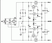
viktor1986 said:Hi
What's your opinion about this amplifier?")
What is good with Lateral MOS, like 2SK1058 / 2SJ162,
is they are easy to parallel, compared to IRF HEXFET and Bipolar power transistors.
What I have read, you don't even have to use any emitter resistors
when parallel several www.renesas.com Laterals ( former Hitachi line ).
I don't think this is true for all lateral MOS.
There are several variants of laterals with different thermal behavior.
In your case you use 0.1 Ohm.
It wont hurt to use emittor resistors anyway
and also makes it much easier to set and measure the Idle Bias Current.
I think 2SK1058 has got considerably HIGHER RDS-on than most power HEXFET.
This also means that they will start clipping maybe already when
Volt Drain-Source is 4-6 volt.
So, when using Lateral MOS instead of vertical IRF HEXFET
you need maybe 3-6 volt higher voltage supply both in V+ V- half.
This makes a total of 6-12 VDC
and so transformer needs to be 4-8 VAC higher.
For example one amp IRF240 / IRF9240 uses 2x30 VAC. ( 60 VAC )
If using 2SK1058 / 2SJ162, maybe need 2X32-2x34 VAC. ( 64-68 VAC )
For same power output.
lineup
Hi
I am currently sort of tinkering with a somewhat similar topology. I have to agree with Mike's comments though. If you replace Q7/Q8 with resistors, they would provide a reference for the second diff pair. If it were me, and my goal was to "linierize" the input diff, I would go for cascode and resistors instead of CCS's.... (J-fets MMMmmmm J-fets....and their high input impeadance ) Cascode is better and the resistors provide a reference for the second stage(Q11, Q12) then maybe R12 can be replace with a CCS for better common mode rejection in the second diff. If R10 in the swap mirror were replaced with a pot, the bias could be adjusted to the correct amount. I have a "homeade amp" that has been working and sounding great for quite some time, I usually just leave it on for days, no problems. It uses a swap mirror for the Q9/Q10 mirror place in this circuit. Speaking of mirrors, I've figured a way to implement a Thompson mirror in the case of the Q9/Q10 mirror for this type of topology that actually works. I love having to rebuild because of an upgrade....but that's DYI.
I am currently sort of tinkering with a somewhat similar topology. I have to agree with Mike's comments though. If you replace Q7/Q8 with resistors, they would provide a reference for the second diff pair. If it were me, and my goal was to "linierize" the input diff, I would go for cascode and resistors instead of CCS's.... (J-fets MMMmmmm J-fets....and their high input impeadance
) Cascode is better and the resistors provide a reference for the second stage(Q11, Q12) then maybe R12 can be replace with a CCS for better common mode rejection in the second diff. If R10 in the swap mirror were replaced with a pot, the bias could be adjusted to the correct amount. I have a "homeade amp" that has been working and sounding great for quite some time, I usually just leave it on for days, no problems. It uses a swap mirror for the Q9/Q10 mirror place in this circuit. Speaking of mirrors, I've figured a way to implement a Thompson mirror in the case of the Q9/Q10 mirror for this type of topology that actually works. I love having to rebuild because of an upgrade....but that's DYI. MikeB said:I think, you should not use the "current mirror" formed by Q7/8. This way the outputv oltage to the 2nd stage is not clearly defined, giving unreliable bias in the 2nd stage.
---------------
EDIT: For a better understanding: This topology needs a voltage output from 1st stage rather than a current output.
CBS240 said:I am currently sort of tinkering with a somewhat similar topology. I have to agree with Mike's comments though.
If you replace Q7/Q8 with resistors, they would provide a reference for the second diff pair.
I agree.
Unfortunately this setup wont work.
There is nothing that sets a stable current through
the important R22 pot in second stage.
Even if you replace Q7 / Q8 with resistors, the current in second stage
will depend on the current source into input differential pair.
And this current source is no good!
Will be like (Power supply Voltage)/(R9+R10).
And if power supply changes under working conditions
the current through R22 pot will change too.
I don't know why you don't use a precise LED CCS to supply Q1 + Q2 ????
Like the one used for Q7 + Q8.
A well defined stable current in second stage is VITAL,
if using only resistor for control of output stage bias!
But is also required very well defined and stable current in input pair
for best performance in all amps using dual transistor differential input.
If using a VBE multiplier instead of R22,
you might get away good with using only input stage CCS
to define Q1+Q2 current precisely and second stage current roughly.
===================================================
Even if there are some other alternatives, I recommend the following:
1. Make a CCS for Q1+Q2 using a RED LED.
This LED should run at like 3-5 mA , set by a resistor from ground.
2. Replace Q7+Q8 with suitable resistors.
To set the current in Q9+Q11+Q10+Q12. See point #4.
3. Replace R22 Pot with a transistor VBE multiplier.
TO126 like MJE340, BD139 will do well.
Also TO92, like 2N5501, BC639, BC635, BC338, BC337 may be used, I think.
This transistor should not / does not have to be placed onto the main heatsink,
as far as I can understand.
4. I would say the current needed in Q10 -> VBE Multiplier -> Q12
to drive output transistors in a good way would be like:
10-15 mA per output pair, 2SK1058 / 2SJ162 ( 600pF / 900pF )
For two pairs like in your schematic, this means something like:
20-30 mA.
The same current will of course run in Q9+Q11.
===================================================
Otherwise, you may keep your circuit basically the same
as what I can see at a very quick look.
It is a good circuit basically with a lot of potential for Hifi performance.
It shows that the designer has quite a bit of knowledge in Audio Amplifiers.
lineup
Lineup Audio Amplifiers
http://lineup.awardspace.com/
Sometime simple is better in both terms of sonic quality and performance. Why not consider the Nelson Pass A40 board with the output design of your choosing? This is a very good sounding amplifier that you can beat the snot out of and count on to run the next time you flip the switch.
I made some with bipolar output stage and I absolutely loved them. Sorry Nelson, I just understand bipolar better than mosfets.
With respect to the schematic you posted...well, it has too many faults. When you do modify it enough to work properly I believe it will have its own colored sonic signature. In the purest sense of audio shouldn't the program remain as close to natural as the original.
Re: !
Now it's OK, except the fact, that output stage bias is highly dependent on supply voltage.
Adam
viktor1986 said:Here is new schematic...
Now it's OK, except the fact, that output stage bias is highly dependent on supply voltage.
Adam
Just don't get this ........
New schematic attachment:
http://www.diyaudio.com/forums/attachment.php?s=&postid=1054782&stamp=1163327250
I don't know why you use 2 resistors R9+R10 to set the current in input stage.
And this current mirrored by Q3-Q4-Q5-Q6.
Such a bias of the input pair Q1+Q2 s really bad, in a HIFI power amp.
And this in combination with only using a variable resistor R22
to set the idle current in output stage,
Sorry, to me it is almost foolish ......
For a mediocre amplifier maybe, but not for high class.
In a preamp we could use regulators, at lower powers and lower voltages.
But using regulators for a power amplifier, at least including the output stage,
is not what I consider a good option.
#################################
What is best and easy solution here?
- Using 2 resistors and an extra dual supply voltage regulator, at 50 Volt or more.
- Using a good normal: RED LED + 1 Transistor CCS
for Q1+Q2 and have a normal power supply.
Why complicate things?
Just to defend your idea from the beginning.
I just don't get it ....
Sorry, viktor.
Regards
lineup
viktor1986 said:Here is new schematic...
New schematic attachment:
http://www.diyaudio.com/forums/attachment.php?s=&postid=1054782&stamp=1163327250
I don't know why you use 2 resistors R9+R10 to set the current in input stage.
And this current mirrored by Q3-Q4-Q5-Q6.
Such a bias of the input pair Q1+Q2 s really bad, in a HIFI power amp.
And this in combination with only using a variable resistor R22
to set the idle current in output stage,
Sorry, to me it is almost foolish ......
For a mediocre amplifier maybe, but not for high class.
In a preamp we could use regulators, at lower powers and lower voltages.
But using regulators for a power amplifier, at least including the output stage,
is not what I consider a good option.
#################################
What is best and easy solution here?
- Using 2 resistors and an extra dual supply voltage regulator, at 50 Volt or more.
- Using a good normal: RED LED + 1 Transistor CCS
for Q1+Q2 and have a normal power supply.
Why complicate things?
Just to defend your idea from the beginning.
I just don't get it ....
Sorry, viktor.
Regards
lineup
A few points:
1) Lateral fets need about 12V Vgs to be at the edge of saturation at their maximum current, 7A. An amplifier with LFETs on the output should therefore have a separate power supply for the driving and input stages that is at least 12V higher than output stage power rail minimum (this is the dip of the ripple waveform at full load), plus whatever voltage drop is generated or required by the actual driver/input stages. This 12V saturation voltage is given as a maximum in the LMOS specs! An extra power supply will have other benefits, too.
2) There is nothing wrong with regulating LMOS idle current with resistor, assuming the differential driver stage current is well defined, and the resistor is VERY well bypassed (think what happens when current limit zeners do their work!). Of course, one could make a proper regulator here (TLxxx) but the problem is getting the temperature coefficient at worst zero. A regular Vbe multiplier will not work here (tempco, even off the ehatsink!), a bit more complexity is needed. The question is, is it required?
3) IS the driver stage current well defined? Well, in the first schematic it was completely undefined. In the second schematic it is dependant on the tail current of the input LTP. This in turn is defined by the positive power rail voltage for this stage. Assuming the power supply IS regulated, then there is nothing terribly wrong with the current mirror used to supply the tail current of the input LTP except that it is really needlessly complicated (and, IIRC, lifted right off a schematic by Dr. Bora Jagodic ). A standard cascode CCS would do better here, and, note to lineup, this is also dependant on the power rail voltage unless the current through the reference is also made constant (which brings us to 'recursion: see under 'recursion'' )
4) Easy paralleling of LMOS is a myth which will be corroborated by anyone who has ever serviced a Hafler amplifier with multiple LMOS pairs. They do share current far better than any other transistor without the addition of source resistors, but you really can't assume 2xLFET with Idmax=7A in parallel, means now Idmax is 14A. It is close, though!
1) Lateral fets need about 12V Vgs to be at the edge of saturation at their maximum current, 7A. An amplifier with LFETs on the output should therefore have a separate power supply for the driving and input stages that is at least 12V higher than output stage power rail minimum (this is the dip of the ripple waveform at full load), plus whatever voltage drop is generated or required by the actual driver/input stages. This 12V saturation voltage is given as a maximum in the LMOS specs! An extra power supply will have other benefits, too.
2) There is nothing wrong with regulating LMOS idle current with resistor, assuming the differential driver stage current is well defined, and the resistor is VERY well bypassed (think what happens when current limit zeners do their work!). Of course, one could make a proper regulator here (TLxxx) but the problem is getting the temperature coefficient at worst zero. A regular Vbe multiplier will not work here (tempco, even off the ehatsink!), a bit more complexity is needed. The question is, is it required?
3) IS the driver stage current well defined? Well, in the first schematic it was completely undefined. In the second schematic it is dependant on the tail current of the input LTP. This in turn is defined by the positive power rail voltage for this stage. Assuming the power supply IS regulated, then there is nothing terribly wrong with the current mirror used to supply the tail current of the input LTP except that it is really needlessly complicated (and, IIRC, lifted right off a schematic by Dr. Bora Jagodic
). A standard cascode CCS would do better here, and, note to lineup, this is also dependant on the power rail voltage unless the current through the reference is also made constant (which brings us to 'recursion: see under 'recursion'' )4) Easy paralleling of LMOS is a myth which will be corroborated by anyone who has ever serviced a Hafler amplifier with multiple LMOS pairs. They do share current far better than any other transistor without the addition of source resistors, but you really can't assume 2xLFET with Idmax=7A in parallel, means now Idmax is 14A. It is close, though!
ilimzn said:A few points:
1) Lateral fets need about 12V Vgs to be at the edge of saturation at their maximum current, 7A. An amplifier with LFETs on the output should therefore have a separate power supply for the driving and input stages that is at least 12V higher than output stage power rail minimum (this is the dip of the ripple waveform at full load), plus whatever voltage drop is generated or required by the actual driver/input stages. This 12V saturation voltage is given as a maximum in the LMOS specs! An extra power supply will have other benefits, too.
An extra PS can be higher voltage, lower current, and have a steady voltage regulator. Have done similar(not with LFET though), but built 2 seperate "DC amplifiers", + & -, to power the driver section. This would make the DC steady, so the input stage bias mirror current would not fluctuate with ripple or rail noise so C3 is not needed. I used a cascaded J-fet CCS for this function instead of mirror.....IMO better.
- Status
- This old topic is closed. If you want to reopen this topic, contact a moderator using the "Report Post" button.
- Home
- Amplifiers
- Solid State
- Opinion about this hi-fi amplifier