Hi all,
This is not in the appropriate section of the forum, sorry i'm not sure where exactly it belongs.
I was wondering if anyone knows of a program that can take a black and white track layout graphic and expand the tracks so there is less no-copper areas? Sure, I could do this myself, but the layout is quite large and there's a tendency for me to expand certain tracks and not others to make my life easier.
Thanks,
Alex
Seems like as good a forum segment as any from my POV...
Why not do them piecewise as you suggest, and only expand the higher-current/lower-impedance segments? With high impedance input stages, there's no real requirement for wide tracks, and you may just increase stray/parasitic capacitance... I favor the approach of handling trace widths individually and increasing the size of low-impedance tracks and not otherwise (perhaps even decreasing high-impedance routes). I certainly don't pretend to be any sort of expert, but this has worked well for me, both in digital and analog arenas...
I sort of tend toward a rule-of-thumb per PCB layout/design, which could probably be approximated as:
trace width ~ amps / sqrt(frequency), though I don't mean to say I'm all that rigorous.
Of course, there are NO absolutes. If this were an incorrect statement, this forum might as well cease to exist (which I hope does NOT happen).
Happy listening!
Hi, thanks for the replies.
The problem I have is that although I like to build amplifiers from the ground up and compare the differences in sound, I am not yet very knowledgeable about how they work, hence i find it quite difficult to work out how wide certain tracks should be compared to others (unless they are power rails).
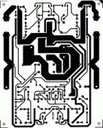
I have attached the current amplifier layout I am building. It's taken from "High End Audio Equipment" Elektor Electronics book, it's almost identical to this:
http://users.otenet.gr/~athsam/power_amplifier_65w_hexfet_eng.htm
though i decided to stick with the layout the book provides.
Anyone built this amplifier design before? any comments?
I think the book probably shows the most efficient layout they could come up with, so perhaps i'll just "fill in" the gaps with areas of copper that are not connected to any part of the circuit just so that my boards won't take days to etch.
Thanks,
Alex
The problem I have is that although I like to build amplifiers from the ground up and compare the differences in sound, I am not yet very knowledgeable about how they work, hence i find it quite difficult to work out how wide certain tracks should be compared to others (unless they are power rails).
I have attached the current amplifier layout I am building. It's taken from "High End Audio Equipment" Elektor Electronics book, it's almost identical to this:
http://users.otenet.gr/~athsam/power_amplifier_65w_hexfet_eng.htm
though i decided to stick with the layout the book provides.
Anyone built this amplifier design before? any comments?
I think the book probably shows the most efficient layout they could come up with, so perhaps i'll just "fill in" the gaps with areas of copper that are not connected to any part of the circuit just so that my boards won't take days to etch.
Thanks,
Alex
Attachments
Hi elaar,
Just keep in mind that copper trace has resistance, be it small, it will have an effect in certain places, particularly those with lots of current. Douglas Self has explained quite well about the need to have the trace of equal distance and resistance from each output device to the negative feedback point of the circuit or you may (or may not) encounter stability issues. It is a good and helpful design tip made by Mr. Self.
Just keep in mind that copper trace has resistance, be it small, it will have an effect in certain places, particularly those with lots of current. Douglas Self has explained quite well about the need to have the trace of equal distance and resistance from each output device to the negative feedback point of the circuit or you may (or may not) encounter stability issues. It is a good and helpful design tip made by Mr. Self.
Hi Elaar,
the layout from the elektor-book looks very familiar to me, i think i built that one about 18 years ago.
I'm not sure about the amp in the link you provided, cannot check for consistency but the pcb looks like something i could come up with.
If i recall correctly the elektor (elektuur) amp used a c-r-c powersupply with 2x 10.000 uf on the pcb.
The amp ran fine in my system for over two years driving a pair of kef cs-7's.
The only hurdle i encountered after i built it was intermittent shorting of the hexfets to the heatsinks, caused by overtightening of the mounting-screws
using silpads.It's also a good idea to deburr the edges of the to0220s to get rid of the sharp edges.
I ended up using aluminum-oxide isolators to get rid of the problem.
With respect to knowledge, i think we're more or less on the same boat, so i'm not sure if i can offer more help.
The elektor-layout worked fine for me, so my suggestion would be to stick to that.
Hope this helps.
With kind regards,
Klaas
elaar said:I am not yet very knowledgeable about how they work, hence i find it quite difficult to work out how wide certain tracks should be compared to others (unless they are power rails).
Thanks,
Alex
Alex - Understood. If you post a schematic, you'll definitely get a lot of mileage from this particular forum, especially in terms of gaining this kind of expertise. One of my favorite parts of amp design is [what I call] quiescent analysis; where you apply the laws of Ohm and Kirchoff, to determine expected bias currents and node voltages, based in great part upon resistor values. Learning to do that was part of what allowed me to begin to create my own designs, as well as to be able to make strategic modifications, including the sort you wish to engage...
Like I said, I'm not the end-all expert, but I for one would be happy to make my best effort to help you analyze a schematic to this end, and I'm sure I'm not alone in that statement. If you're building amps in the first place, and know how to test them and get them working correctly, you're nearly there already! Even ground-up building of existing designs requires some analysis & troubleshooting ability in most cases.
-Jonathan
re: your board
Personally, I would just expand the copper area (black) near the left & right edges ... up to but not including your mount holes in the corners.
If that area is to be your "ground plane", then no problem with the added "stray capacitance" ... if not, then not.
I would do this "by hand" with any of the built in paint programs (Apple > Apple Works > Paint, etc.)
acoustixman said:If you post a schematic,
OK, Duh on me. I just realized you had posted this link. I'm looking at it now...
Layout Manipulation
Alex
There are a couple of layout programs that can be used to maipulate the layout once it has been scanned.
There are more that will allow the manipulation of gerbers.
Most of the tools are linked to an layout package.
The question is what package are you using for the layout? Then someone may have a tool that will allow manipulation.
Brian
bscally....There are a couple of layout programs that can be used to maipulate the layout once it has been scanned.
Do you know which programs are these?
Thanks
Alright; to better answer your initial question;
I always use "ExpressPCB"... It's a freeware CAD program inclusive of schematic and PCB layout software, with file linkage for built-in PCB design proofing / evidence (alas, no auto-routing)... It's very easy software to learn and once you complete your PCB layout on the screen, you simply electronically submit with a nominal fee via credit card, choosing whether you want solder masks and silkscreens at time of submittal. A few days later, your PCBs arrive at your door by UPS. I'm not sure whether you can get them to the UK...I'd wager you can though - I personally use Exicon lateral MOSFETs exclusively in output stages of my power amp designs, and they are sourced from Profusion PLC in the UK. They always come by UPS. The software I mention can be downloaded freely from:
ExpressPCB dot com
MY OWN RULES OF THUMB (take this with grains of salt if desired): I would personally make the supply rail and ground traces huge (3-4mm or better if possible, including connections to 'on-board' rail filter capacitors), as well as the drain and source traces about the MOSFETs. Working backward, the predrivers (Q10-Q11) are biased at about 13mA (which incidentally comes awfully close to the DC SOA boundaries for these devices at 35V), and this requires much less width (perhaps 1.5-2mm) for the collector and emitter traces here (including the entire path between the rails of course in each case here). Excess width will only increase stray capacitance, from here on back in the layout. If you are generating a new layout to suit yourself, bear in mind that excess length will similarly increase stray inductance, and this is of extreme importance in the area of MOSFET gates, which are capacitive and you will have a resonant system, especially when so tightly-laced as in a Sziklai/CF configuration such as this. From the predriver bases on back, the traces need be no larger than (1-1.25mm) and the smaller the faster.
<SOAPBOX>
----------------------------------------------------
On this schematic design... This looks like a good design from a symmetry perspective (I always utilize symmetrical approaches). Note that in the physical assembly, you'd be best off NOT providing thermal contact from Q12-Q13 back to Q8,Q10, and Q11. It is critical that Q8 thermally track Q10-Q11, but may be almost as important that these three NOT track Q12 and Q13.
I see some potential risks here though...
(1) of BIGTIME CONCERN from my POV: There is NO current limiting for the output devices. If there is a short circuit here, the MOSFETs may instantly be considered junk. Those fuses will only serve to make you unduly confident. It takes an ETERNITY for fuses to heat up, melt and open the circuit, on transistor terms. Those MOSFETs could fail 100 times before the fuses ever act. In fact the fuses will only open after the MOSFETs convert themselves to useless blobs of metalloid, and are therefore only protecting your power supply, wiring, and board traces (if you're lucky). I recommend re-working the design and utilizing a foldback limiting scheme.
(2) The second biggest problem I see right off is using HEXFETs in this type of SZIKLAI/CF output configuration. HEXFETs like to act like switches (and are therefore perfect for class-D designs) and this amp may be finicky and 'tight-wound' with regard to possible oscillations, especially with only 15 ohm "gate stoppers", although this may be slightly mitigated by the ~3dB gain in this stage (CF groups would offer infinite gain if they could). I always use 470 series ohms for MOSFET gate drive in audio designs to prevent ringing, which becomes increasingly important with paralleled output devices. You could be well-advised to investigate the LATERAL MOSFET alternative (just mind the pinouts - they are different from V-MOS/HEXFETS in some packages), especially since some of the best ones (IMHO) come from your country as I have mentioned:
ProfusionPLC dot com
(3) I notice that the [apparently] sole mode of compensation (besides inherent Miller capacitance in Q7, Q9, Q10, Q11, Q12, Q13) utilized is in the form of Zobel bandwidth limiting in the diff amp tails. This is not itself a problem, but this circuit has very high open-loop gain to worry about, especially with the small-value ballast resistors throughout... The diff amp may sit back and allow the HARD local feedback in the Q10-Q13 neighborhood to ring on transients often found in modern music sources. This would cause the amp to lose focus and precision, and could seriously reduce the joy of the listening experience.
(4) Personally, I would probably increase the DA ballast resistors (R8-R11) to increase the dynamic range. Perhaps even 10-fold (to 220 ohms). This would decrease the open-loop gain, make the amp more stable, and cause the the diff amp to be much better able to dynamically control the Sziklai output (as well as reducing the requirement for precise component matching to boot). As it stands with 2mA of DA bias upon 22-ohm ballast, the input dynamic range is approximately 44mV (where at this error level two diagonally opposed transistors, Q1,Q4 OR Q2,Q3, are cut off completely). This would be 0.44V with the modification I suggest. Such low dynamic range can cause the diff amp to lose control under transient conditions, and the amplifier will slew (bad; this represents the amplifier's last-ditch and non-linear effort to restore waveform abidance). This does not take into account that this should actually be divided twofold to account for bias level of Q7 and Q9, which will respectively be switched off (and thus slewing the output) as soon as that 1.2V diminishes to about 0.6V, which will be at an input dynamic level of 22mV. IMO, this is quite inadequate considering that line level music may have 1V peaks, 45 times greater than that which makes this amplifier slew. This will not be a problem at steady state, but with transients such as string plucking or modern synthesized waveforms, this amp will slew all over the place since the bandwidth is finite. I wouldn't drive my car without shock absorbers any more than I would produce such low dynamic range in my own designs. All this would be out the window if the tail end of the amplifier could respond absolutely instantaneously, and not ring, but there is definitely and always a finite propagation time through the circuit (hence the requirement for bandwidth specification) and music can happen very quickly (unless you're building it strictly for low-frequency service in a multi-amp system). I have never been more pleasurably engaged in music listening than when listening to high dynamic range designs like I describe. Though I have never personally auditioned one, the 'essential' Leach amp is such a design available for comparison, and he offers good descriptions of rationale on his web page:
Leach Amp Design Page
</SOAPBOX>
----------------------------------------------------
I am gravely sorry to be so lengthy and so potentially off-topic (I'm probably developing a bad reputation around here for going off on tangents ), but I fear this design could be a real BEAR to tweak into existence for at least a couple of these lines of reasoning. I only sincerely hope everyone can enjoy the beautiful sonic elegance and effortlessly transparent crispness of a high-dynamic range amplifier at some point in their lifetime. I can personally testify as a musician that such amplifiers are themselves a testament to the intrinsic beauty of music, and on its [music's] own terms of freedom, joy, and artistic appeal. I think it is high-gain, low dynamic range amplifiers that gave transistors a bad name (such as having a harsh and unfocused sound relative to valves) in the first place.
As always, happy listening!!
I always use "ExpressPCB"... It's a freeware CAD program inclusive of schematic and PCB layout software, with file linkage for built-in PCB design proofing / evidence (alas, no auto-routing)... It's very easy software to learn and once you complete your PCB layout on the screen, you simply electronically submit with a nominal fee via credit card, choosing whether you want solder masks and silkscreens at time of submittal. A few days later, your PCBs arrive at your door by UPS. I'm not sure whether you can get them to the UK...I'd wager you can though - I personally use Exicon lateral MOSFETs exclusively in output stages of my power amp designs, and they are sourced from Profusion PLC in the UK. They always come by UPS. The software I mention can be downloaded freely from:
ExpressPCB dot com
MY OWN RULES OF THUMB (take this with grains of salt if desired): I would personally make the supply rail and ground traces huge (3-4mm or better if possible, including connections to 'on-board' rail filter capacitors), as well as the drain and source traces about the MOSFETs. Working backward, the predrivers (Q10-Q11) are biased at about 13mA (which incidentally comes awfully close to the DC SOA boundaries for these devices at 35V), and this requires much less width (perhaps 1.5-2mm) for the collector and emitter traces here (including the entire path between the rails of course in each case here). Excess width will only increase stray capacitance, from here on back in the layout. If you are generating a new layout to suit yourself, bear in mind that excess length will similarly increase stray inductance, and this is of extreme importance in the area of MOSFET gates, which are capacitive and you will have a resonant system, especially when so tightly-laced as in a Sziklai/CF configuration such as this. From the predriver bases on back, the traces need be no larger than (1-1.25mm) and the smaller the faster.
<SOAPBOX>
----------------------------------------------------
On this schematic design... This looks like a good design from a symmetry perspective (I always utilize symmetrical approaches). Note that in the physical assembly, you'd be best off NOT providing thermal contact from Q12-Q13 back to Q8,Q10, and Q11. It is critical that Q8 thermally track Q10-Q11, but may be almost as important that these three NOT track Q12 and Q13.
I see some potential risks here though...
(1) of BIGTIME CONCERN from my POV: There is NO current limiting for the output devices. If there is a short circuit here, the MOSFETs may instantly be considered junk. Those fuses will only serve to make you unduly confident. It takes an ETERNITY for fuses to heat up, melt and open the circuit, on transistor terms. Those MOSFETs could fail 100 times before the fuses ever act. In fact the fuses will only open after the MOSFETs convert themselves to useless blobs of metalloid, and are therefore only protecting your power supply, wiring, and board traces (if you're lucky). I recommend re-working the design and utilizing a foldback limiting scheme.
(2) The second biggest problem I see right off is using HEXFETs in this type of SZIKLAI/CF output configuration. HEXFETs like to act like switches (and are therefore perfect for class-D designs) and this amp may be finicky and 'tight-wound' with regard to possible oscillations, especially with only 15 ohm "gate stoppers", although this may be slightly mitigated by the ~3dB gain in this stage (CF groups would offer infinite gain if they could). I always use 470 series ohms for MOSFET gate drive in audio designs to prevent ringing, which becomes increasingly important with paralleled output devices. You could be well-advised to investigate the LATERAL MOSFET alternative (just mind the pinouts - they are different from V-MOS/HEXFETS in some packages), especially since some of the best ones (IMHO) come from your country as I have mentioned:
ProfusionPLC dot com
(3) I notice that the [apparently] sole mode of compensation (besides inherent Miller capacitance in Q7, Q9, Q10, Q11, Q12, Q13) utilized is in the form of Zobel bandwidth limiting in the diff amp tails. This is not itself a problem, but this circuit has very high open-loop gain to worry about, especially with the small-value ballast resistors throughout... The diff amp may sit back and allow the HARD local feedback in the Q10-Q13 neighborhood to ring on transients often found in modern music sources. This would cause the amp to lose focus and precision, and could seriously reduce the joy of the listening experience.
(4) Personally, I would probably increase the DA ballast resistors (R8-R11) to increase the dynamic range. Perhaps even 10-fold (to 220 ohms). This would decrease the open-loop gain, make the amp more stable, and cause the the diff amp to be much better able to dynamically control the Sziklai output (as well as reducing the requirement for precise component matching to boot). As it stands with 2mA of DA bias upon 22-ohm ballast, the input dynamic range is approximately 44mV (where at this error level two diagonally opposed transistors, Q1,Q4 OR Q2,Q3, are cut off completely). This would be 0.44V with the modification I suggest. Such low dynamic range can cause the diff amp to lose control under transient conditions, and the amplifier will slew (bad; this represents the amplifier's last-ditch and non-linear effort to restore waveform abidance). This does not take into account that this should actually be divided twofold to account for bias level of Q7 and Q9, which will respectively be switched off (and thus slewing the output) as soon as that 1.2V diminishes to about 0.6V, which will be at an input dynamic level of 22mV. IMO, this is quite inadequate considering that line level music may have 1V peaks, 45 times greater than that which makes this amplifier slew. This will not be a problem at steady state, but with transients such as string plucking or modern synthesized waveforms, this amp will slew all over the place since the bandwidth is finite. I wouldn't drive my car without shock absorbers any more than I would produce such low dynamic range in my own designs. All this would be out the window if the tail end of the amplifier could respond absolutely instantaneously, and not ring, but there is definitely and always a finite propagation time through the circuit (hence the requirement for bandwidth specification) and music can happen very quickly (unless you're building it strictly for low-frequency service in a multi-amp system). I have never been more pleasurably engaged in music listening than when listening to high dynamic range designs like I describe. Though I have never personally auditioned one, the 'essential' Leach amp is such a design available for comparison, and he offers good descriptions of rationale on his web page:
Leach Amp Design Page
</SOAPBOX>
----------------------------------------------------
I am gravely sorry to be so lengthy and so potentially off-topic (I'm probably developing a bad reputation around here for going off on tangents
), but I fear this design could be a real BEAR to tweak into existence for at least a couple of these lines of reasoning. I only sincerely hope everyone can enjoy the beautiful sonic elegance and effortlessly transparent crispness of a high-dynamic range amplifier at some point in their lifetime. I can personally testify as a musician that such amplifiers are themselves a testament to the intrinsic beauty of music, and on its [music's] own terms of freedom, joy, and artistic appeal. I think it is high-gain, low dynamic range amplifiers that gave transistors a bad name (such as having a harsh and unfocused sound relative to valves) in the first place. As always, happy listening!!
Hi, wow thanks for the replies, now where do I start?
Firstly, thanks for the mention of Douglas Self CBS240, I looked up his website and found many of the articles an interesting read.
Kvholio: I didn't realise this was such an old design, although the hexfets weren't easy to get And yes you're right, there's also large caps on the main pcbs (as mentioned later). As you suggested, I'm going to stick with the layout they supply and fill in gaps with sections of copper which aren't connected to anything, just because otherwise my boards don't etch too well if there's too much copper to remove.
acoustixman: Thanks for the pcb design program recommendation, i'll definitely give it a try if they ship to the UK. Also thanks for the amplifier design criticism, it seems that whatever amplifier I decide to build there's always some design problems with it, anyone know of a perfect amplifier I can build?
Unfortunately, I don't know enough about amplifiers to truly understand your points
Re: No current limiting for short circuits: The book states that "The hexfets have an inherent current limitation by virtue of their positive temperature coefficient: when the device gets hot, it's drain-source resistance rises and this reduces the current through it. The fuses and this property provide adequate protection against brief short-circuits.". Also that these hexfes can handle peak currents of up to 75A. Do you think then that this protection is over exaggerated and not sufficient?
Even with the other design problems you state, would this still be a reasonable amplifier to make or am I wasting my time? I've spent quite a while matching the transistors and sourcing some parts unfortunately. Perhaps like you hinted, I could use these for the bass speakers in a future active speaker build.
I'm off to read the leach amplifier link and have a beer.
Thanks very much for the comments
Firstly, thanks for the mention of Douglas Self CBS240, I looked up his website and found many of the articles an interesting read.
Kvholio: I didn't realise this was such an old design, although the hexfets weren't easy to get
And yes you're right, there's also large caps on the main pcbs (as mentioned later). As you suggested, I'm going to stick with the layout they supply and fill in gaps with sections of copper which aren't connected to anything, just because otherwise my boards don't etch too well if there's too much copper to remove.acoustixman: Thanks for the pcb design program recommendation, i'll definitely give it a try if they ship to the UK. Also thanks for the amplifier design criticism, it seems that whatever amplifier I decide to build there's always some design problems with it, anyone know of a perfect amplifier I can build?
Unfortunately, I don't know enough about amplifiers to truly understand your points
Re: No current limiting for short circuits: The book states that "The hexfets have an inherent current limitation by virtue of their positive temperature coefficient: when the device gets hot, it's drain-source resistance rises and this reduces the current through it. The fuses and this property provide adequate protection against brief short-circuits.". Also that these hexfes can handle peak currents of up to 75A. Do you think then that this protection is over exaggerated and not sufficient?
Even with the other design problems you state, would this still be a reasonable amplifier to make or am I wasting my time? I've spent quite a while matching the transistors and sourcing some parts unfortunately. Perhaps like you hinted, I could use these for the bass speakers in a future active speaker build.
I'm off to read the leach amplifier link and have a beer.
Thanks very much for the comments
elaar said:acoustixman: Thanks for the pcb design program recommendation, i'll definitely give it a try if they ship to the UK. Also thanks for the amplifier design criticism, it seems that whatever amplifier I decide to build there's always some design problems with it, anyone know of a perfect amplifier I can build?
Unfortunately, I don't know enough about amplifiers to truly understand your points
Fortunately for the passionate audio enthusiast, a shortage of knowledge is always a temporary condition!
My personal amplifier favorites are as I described in my too-long post, with the addition of cascode stages upon non-common collectors. The combination of ultra-quick and lower-gain makes for a tear-jerking encounter with my favorite songs. It seems like nirvana to me and I would love to claim that I have designed and built the perfect amplifier, but alas, such a device does not exist. I think the union of good forces (such as those of us who ask questions and give answers in this forum) with possible designs is the best path to enlightenment. Let's keep it an art!
Re: No current limiting for short circuits: The book states that "The hexfets have an inherent current limitation by virtue of their positive temperature coefficient...*snip*...Do you think then that this protection is over exaggerated and not sufficient?
Definitely. The fuses take orders of magnitude longer to blow than the transistors; "brief" is a very relative term. You are correct about the temperature coefficient. This fact does more for SF designs in terms of bias stability, and also helps to maintain balanced current sharing among paralleled FETs (HEX or otherwise). Unfortunately, a dead short on the circuit will not be served by this mode of 'protection'. The transistor has a job to do, and its boss is the diff amp. If it's being told to raise the voltage of ground (due to a short) it will try until it literally smokes (milliseconds or less); soon after that, the fuse will blow (seconds). This current would be infinite if the power plant was willing to sell you that much and all other things in between were similarly providential (transmission wire resistance is the only actual reason to the contrary). It's a case of "If your boss told you to jump off a cliff, would you do it?" and the MOSFET would obediently say "YES, OF COURSE I WOULD! what a silly question!
"FET positive temperature coefficients are not at all comparable to PTC thermistor current limiters, which DO provide this sort of protection. I have blown HEXFETs with short circuits with and without fuses. If I were you I'd skip the fuses altogether since they also have temperature coefficients (generally positive to resistance), and this will directly impact the source degeneration resistance of the MOSFETs, and thus the fuses will be 'vocal participants' in dynamic audio performance.

Even with the other design problems you state, would this still be a reasonable amplifier to make or am I wasting my time?
I'm off to read the leach amplifier link and have a beer.
Thanks very much for the comments
Cheers! I am presently inspired by your suggestion of a beer...

The short answer is YES. If I can offer any benefit at all to fellow enthusiasts, I am to be most pleased. I would say do it, if you possess the essential resources (time and money). The amp that is completely not worth exploring exists no more than the perfect one. In your position I would do it, while definitely making the modifications I suggested - I think this would produce an amp capable of producing a striking degree of crisp focus in the sound field, which is to be highly appreciated. Obviously this stuff is subjective and meant to be fun. I'm not trying to win any arguments or assume a contest-deciding expertise, just to preempt frustration and dissapointment.
 My comments were based on the fact that this amp appears to include several segments which EACH tend to carry a reputation for being finicky. Overall the concept is a sound one, if you will pardon the gross pun. Most of my commentary aims toward mere resistance value changes (generally to increase) rather than undermining the topology. If built like I suggest, I see no reason to expect it to be limited to bass performance. I would be interested to see alternate commentary from some of the more esteemed experts here than myself...
Here's a suggestion; Try it without what I've suggested, and then try it with... I'd wager you'll notice, and that's probably the best way to not only determine whether I'm full of !@#$, but also to gain ever-more knowledge.
BTW; Leach represents a 'rather extreme' (can I say that oxymoron?) case of "dynamic range == first priority" (with 300 ohms of DA ballast instead of this design's 22 ohms). I had to read his description about 10 times, but I was sold once I got it. The differential amplifier and second stage sections are where to concentrate a comparison... The extra transistors and stuff toward the rails in the diff amps are very elegant cascode devices for maintaining constant voltage at the collectors of the "core four". This produces a lightening-quick transient response by eliminating the Miller effect. I use similar configurations in all my designs. Unlike Leach, I prefer active current sources for DA biasing (to increase CMRR), pretty much the same as this design you are considering.
Enjoy!
I have also been using express pcb, but have switched over to eagle about 4 days ago... I could just never get the hang of it... now its like , doh, its so easy... getting much neater pcb layouts, healthier cleaner looking traces... basicaly I don't mess with adding the whole schematic etc.. I just go straight to a new board, click add and select my component, double click it and paste it where I want it... was so simple, yet so hard to figure out... all the basic capacitors and resistors are in the library called rcl.... remember that, as it will be the first thing you need to find in all likleyhood...
Nordic said:I have also been using express pcb, but have switched over to eagle about 4 days ago...*snip*
Eagle, you say... Hmmm... Any relationship to Eagle non-inductive wirewound resistors? Maybe I'll check this out. I just have such a connection to ExpressPCB, and have not *yet* been dissapointed... I do like how easy it is to create 'custom' componentry in ExPCB.
Amen to your signature, Nordic. I am such a time-consumer for that very reasoning... But we both know it's in jest, don't we?! The world would probably have ceased its rotation (or something so inconceivable) a while back if everyone always used cookie cutters!
elaar->
Another thought... I think I mentioned that I generally prefer source follower layouts (over the complementary feedback design you are considering). I just thought I'd mention why even though off-topic...
If the MOSFETs are used as source-followers, the predriver stage should be decoupled from the output rail, and the emitter degeneration resistance (R28+R29 in your case, over which the bias voltage is constantly applied) is only connected to the two predrivers and would then be in class-A mode (never going into cutoff). The predriver emitters (rather than the collectors) drive the MOSFET gates, and the predriver emitters will 'glide' where they need to be (courtesy of global feedback) to get the FET sources to the target voltage. Essentially a Darlington approach rather than a Sziklai one. [This is analogously true if you prefer bipolar outputs.]
Anyway, the remark toward which I'm working is that I follow Leach's approach of feedback; since the predrivers are decoupled from the output rail, the point between their resistors is a source of HF feedback. With a series cap+resistor from there to the inverting input, the HF (say 150kHz) and above transients are quickly vented back instead of waiting to gather this information from the output rail. The phase margin is thus improved. With proper gate-stoppers on MOSFETs there is a low-pass RC filter, which limits their speed (hundreds of kHz). With bipolar transistors, a similar effect is due to 'minority carrier injection'. C8 in your circuit serves to reduce this effect in the predrivers, but is obviated in the approach I describe since the predrivers are converted to class-A operation.
In the graphic attached: The left-hand portion shows your circuit's output segment, inclusive of the modifications I suggest there. The right-hand portion is my typical approach. C16+C17 functionally replace your C5, reducing the closed-loop gain to around unity at extreme frequencies (I think this just keeps the circuit from responding to stray RF), except I take this from the VA stage (seems to also improve the phase margin). C18+R36 form the essence of this point, supplying high frequency information from a node-point which is only available in this approach, between the predrivers. R37+R38+C19 cause the MOSFET feedback to roll off, yielding 'ultra-audio responsibility' solely to the predrivers. The crossover point in this case is around 120kHz. The results I have enjoyed include a hair-raising transient response, with very high Nyquist stability (no oscillations, except when I make mistakes like I did recently... ). D7+D9 are a good choice in general. They are Zener diode pairs, in anti-series, serving to limit applied gate voltage (MOSFETs don't like excess gate voltage very much). They generally don't participate in the circuit, but the're about 1/50 the price of the MOSFETs I use. To a certain extent they actually legitimize the PTC approach to current limiting somewhat <in LATERAL MOSFETs>.
Happy listening!!
Another thought... I think I mentioned that I generally prefer source follower layouts (over the complementary feedback design you are considering). I just thought I'd mention why even though off-topic...
If the MOSFETs are used as source-followers, the predriver stage should be decoupled from the output rail, and the emitter degeneration resistance (R28+R29 in your case, over which the bias voltage is constantly applied) is only connected to the two predrivers and would then be in class-A mode (never going into cutoff). The predriver emitters (rather than the collectors) drive the MOSFET gates, and the predriver emitters will 'glide' where they need to be (courtesy of global feedback) to get the FET sources to the target voltage. Essentially a Darlington approach rather than a Sziklai one. [This is analogously true if you prefer bipolar outputs.]
Anyway, the remark toward which I'm working is that I follow Leach's approach of feedback; since the predrivers are decoupled from the output rail, the point between their resistors is a source of HF feedback. With a series cap+resistor from there to the inverting input, the HF (say 150kHz) and above transients are quickly vented back instead of waiting to gather this information from the output rail. The phase margin is thus improved. With proper gate-stoppers on MOSFETs there is a low-pass RC filter, which limits their speed (hundreds of kHz). With bipolar transistors, a similar effect is due to 'minority carrier injection'. C8 in your circuit serves to reduce this effect in the predrivers, but is obviated in the approach I describe since the predrivers are converted to class-A operation.
In the graphic attached: The left-hand portion shows your circuit's output segment, inclusive of the modifications I suggest there. The right-hand portion is my typical approach. C16+C17 functionally replace your C5, reducing the closed-loop gain to around unity at extreme frequencies (I think this just keeps the circuit from responding to stray RF), except I take this from the VA stage (seems to also improve the phase margin). C18+R36 form the essence of this point, supplying high frequency information from a node-point which is only available in this approach, between the predrivers. R37+R38+C19 cause the MOSFET feedback to roll off, yielding 'ultra-audio responsibility' solely to the predrivers. The crossover point in this case is around 120kHz. The results I have enjoyed include a hair-raising transient response, with very high Nyquist stability (no oscillations, except when I make mistakes like I did recently...
). D7+D9 are a good choice in general. They are Zener diode pairs, in anti-series, serving to limit applied gate voltage (MOSFETs don't like excess gate voltage very much). They generally don't participate in the circuit, but the're about 1/50 the price of the MOSFETs I use. To a certain extent they actually legitimize the PTC approach to current limiting somewhat <in LATERAL MOSFETs>.Happy listening!!
Attachments
JW,
I happened by accident to discover this thread and more pointly this reply of yours. I have some questions if I may:
1) Should C5 in the original schematic not be used/installed?
2) Why were the collector resistors R27 and R30 removed?
3) Could C18 be as low as 10p0?
4) Is the R37+R38+C19 120Khz rolloff calculated using standard 12db filter formula?
5) Are you aware you have two C19's in the schematic?
6) What is the RC time constant of R27+C19 to Quiet ground?
7) Assuming one cannot use a Bipolar for C19(+R27), what way would the + of an electrolytic capacitor for C19 face?
8) If one had normally used a 33K0 resistor in the feedback to the input diff pair, one normally uses the same same value, 33K0 in seriers with the input diff pair signal input. The 33k) value is not gixed as many designs aso use 22k0 in both places. I know the original schematic does not follow that practice and my following question is ignoring the orignal schematic that was of discussion in the thread. The question is assuming as an example one wants to follow this same design practice of using the same resistance value on the feedback as used for the input signal to the diff pair, what calculation would you use to ensure the same value for the feedback changes you provided?
Regards,
John L. Males
Willowdale, Ontario
Canada
17 November 2006 14:11
I happened by accident to discover this thread and more pointly this reply of yours. I have some questions if I may:
acoustixman said:elaar->
In the graphic attached: The right-hand portion is my typical approach. C16+C17 functionally replace your C5, reducing the closed-loop gain to around unity at extreme frequencies (I think this just keeps the circuit from responding to stray RF), except I take this from the VA stage (seems to also improve the phase margin). C18+R36 form the essence of this point, supplying high frequency information from a node-point which is only available in this approach, between the predrivers. R37+R38+C19 cause the MOSFET feedback to roll off, yielding 'ultra-audio responsibility' solely to the predrivers. The crossover point in this case is around 120kHz. The results I have enjoyed include a hair-raising transient response, with very high Nyquist stability (no oscillations, except when I make mistakes like I did recently...
Happy listening!!
1) Should C5 in the original schematic not be used/installed?
2) Why were the collector resistors R27 and R30 removed?
3) Could C18 be as low as 10p0?
4) Is the R37+R38+C19 120Khz rolloff calculated using standard 12db filter formula?
5) Are you aware you have two C19's in the schematic?
6) What is the RC time constant of R27+C19 to Quiet ground?
7) Assuming one cannot use a Bipolar for C19(+R27), what way would the + of an electrolytic capacitor for C19 face?
8) If one had normally used a 33K0 resistor in the feedback to the input diff pair, one normally uses the same same value, 33K0 in seriers with the input diff pair signal input. The 33k) value is not gixed as many designs aso use 22k0 in both places. I know the original schematic does not follow that practice and my following question is ignoring the orignal schematic that was of discussion in the thread. The question is assuming as an example one wants to follow this same design practice of using the same resistance value on the feedback as used for the input signal to the diff pair, what calculation would you use to ensure the same value for the feedback changes you provided?
Regards,
John L. Males
Willowdale, Ontario
Canada
17 November 2006 14:11
Correction and Addendum to 17 November 2006 14:11 Posting
Correction for typo and parallel not series use of 33K0 8 should read:
8) If one had normally used a 33K0 resistor in the feedback to the input diff pair, one normally uses the same same value, 33K0 in parallel with the input diff pair signal input. The 33k0 value is not fixed as many designs also use respectively 22k0 in both places. I know the original schematic does not follow that practice and my following question is ignoring the original schematic that was of discussion in the thread. The question is assuming as an example one wants to follow this same design practice of using the same resistance value on the feedback as used in parallel for the input signal to the diff pair, what calculation(s) would you use to ensure the same value for the feedback changes you provided as for the parallel input resistance to the diff pair?
Addition on my mind list that I forgot to obviously ask:
9) What calculation(s) are used to determine the feedback gain of your feedback circuit? The traditional feedback gain calculation Rfb/Rgnd, i.e. 33k0/1k0 = 33 or 22k0/1k0 = 22, or 27k0/1k0 = 27 seem to be the common values used.
Regards,
John L. Males
Willowdale, Ontario
Canada
19 November 2006 11:31
keypunch said:
8) If one had normally used a 33K0 resistor in the feedback to the input diff pair, one normally uses the same same value, 33K0 in seriers with the input diff pair signal input. The 33k) value is not gixed as many designs aso use 22k0 in both places. I know the original schematic does not follow that practice and my following question is ignoring the orignal schematic that was of discussion in the thread. The question is assuming as an example one wants to follow this same design practice of using the same resistance value on the feedback as used for the input signal to the diff pair, what calculation would you use to ensure the same value for the feedback changes you provided?
Regards,
John L. Males
Willowdale, Ontario
Canada
17 November 2006 14:11
Correction for typo and parallel not series use of 33K0 8 should read:
8) If one had normally used a 33K0 resistor in the feedback to the input diff pair, one normally uses the same same value, 33K0 in parallel with the input diff pair signal input. The 33k0 value is not fixed as many designs also use respectively 22k0 in both places. I know the original schematic does not follow that practice and my following question is ignoring the original schematic that was of discussion in the thread. The question is assuming as an example one wants to follow this same design practice of using the same resistance value on the feedback as used in parallel for the input signal to the diff pair, what calculation(s) would you use to ensure the same value for the feedback changes you provided as for the parallel input resistance to the diff pair?
Addition on my mind list that I forgot to obviously ask:
9) What calculation(s) are used to determine the feedback gain of your feedback circuit? The traditional feedback gain calculation Rfb/Rgnd, i.e. 33k0/1k0 = 33 or 22k0/1k0 = 22, or 27k0/1k0 = 27 seem to be the common values used.
Regards,
John L. Males
Willowdale, Ontario
Canada
19 November 2006 11:31
- Status
- This old topic is closed. If you want to reopen this topic, contact a moderator using the "Report Post" button.
- Home
- Amplifiers
- Solid State
- Track layout design