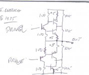
During my years in audio I required a higher voltage output stage than could be provided by the then available output transistors
so I developed the attached output stage and during the last thirty years i have used it several times with success as i have never seen it used else where i would apreciate your comments and thoughts re this attached sketch
Please remember that this was developed in the days of the 2n3055/2n2955 the modern devices of today were but a dream
and i suppose could be used with the modern devices for the killowatt amps etc
all comments are welcome regards Trev
Attachments
Looks similar to the cascode output stage used in the Leach SuperAmp (aka the Double-Barelled Amplifier)
http://users.ece.gatech.edu/~mleach/superamp/
http://users.ece.gatech.edu/~mleach/superamp/
Hi latala
This circuit is very clever, on paper it looks like doubling the maximum Vce of output transistors. Are there any benefits campairing to vintage series connection (as in quoted Leach)? Definitely on scheamtic it looks more clever and simpler, but what more?
best regards
Adam
This circuit is very clever, on paper it looks like doubling the maximum Vce of output transistors. Are there any benefits campairing to vintage series connection (as in quoted Leach)? Definitely on scheamtic it looks more clever and simpler, but what more?
best regards
Adam
i havnt seen the super leach but if you study this you will find its not a cascode at all but a pair of series connected complimentary transistors with drive taken from both sides of the driver
regards Trev the 1975 ref is from an old sketch pad thaty i found in the garage
believe me if you saw my garage you could believe i havent been there since then
there are disadvantages such as twice the normal sat voltage per side but thats a small price to pay
the seies conncted resistor are to balance out the supply voltage across the series connected devices
i have a few more quirky designs such as these is there any intersest in these
i would like to see them in the worlld rather than just fade away
regards trev
the out put stage was as stable as the conventional darlington pair type and provided that the vas stage is correctly compensated no problems at all were encountered
from memory the circuit was a conventional dif pair feeding a common emiter vas amp with a pair of transistors connected a a constant current load bias being set via a rubber diode
i have always tended to run the diff front pair at about 0.5 ma per device with 5 ma on the vas stage
compensation around the vas stage being a nominal 100 pf
but here the compensation cap is from the collector of the vas amp to the base of the feedback leg of the diff pair
this i have found always sonded nicer smoother
also the drive from the vas stage to the driver transistors was via a typical 220 resistor
this improved recovery from over drive conditions
as i said at the begining this schematic is more of use to the builder who happens to have the transistors in the junk box etc
i will be pleased to discuss or supply a more complete schematic if required
i dont know much about pcb programs can you people out there read qroute 3 schematics
regards trev
latala said:i have always tended to run the diff front pair at about 0.5 ma per device with 5 ma on the vas stage
The bandwidth gain product is lower at smaller currents in most small signal devices. How does this affect the operation of the diff pair? I am fond of SOT-23 transistors and lower currents is helpful here.
Hello Trev,
I have strong doubts that this series connection will divide their Uce equal! The both transistors and Re s had to be very equal and this over a broad range of current and voltage.
Functional You switched two high current sources together, with
a load of 5k.....this arrangement has much more amplification than a VAS.
Regards
Heinz
Hi Trev,
That's very similar as seen in the Bryston 4B. It's been around for a long, long time. They used 2N3773 and 2N6609 as outputs, MJE15028 and compliment as the driver.
Apparently it's stable, and it works. The biggest difference is the polarity of the driver transistor.
-Chris
That's very similar as seen in the Bryston 4B. It's been around for a long, long time. They used 2N3773 and 2N6609 as outputs, MJE15028 and compliment as the driver.
Apparently it's stable, and it works. The biggest difference is the polarity of the driver transistor.
-Chris
thr bryston 48
does any one out ther have a schematic or at least a partial on the output stage as i would like to see it re the output configuration as for matching the output devices no special attempts were made the emittor resistors on the output devices are essential here as they act as the stabalisers in this case as for balancing the voltage split this is the function of the 10 k resistors wich tend to swamp any leakage differances in the output devices
as i say it works and works well
i have suggested it as a scheme to allow the use of available devices at a lower cost also remember that the device dissipation will be half of a singe device per normal output stage at any given power
regards trev
The current Bryston uses the phase splitter driver transistor with one of each polarity output, but the outputs are in parallel.
http://www.bryston.ca/BrystonSite05/pdfs/SSTAmplifiers/4b+7bSST-SSB-SCH-6_20041013.pdf
http://www.bryston.ca/BrystonSite05/pdfs/SSTAmplifiers/4b+7bSST-SSB-SCH-6_20041013.pdf
 Unusual circuit...what's it all about?
If the purpose is to allow higher supply voltages by dividing the supply across two transistors then to work well the two transistors are very well matched and the driver has to have very high beta and the resistors must be closely matched. Sort of a difficult way to achieve the goal I reckon.
Any difference in collector currents of the two power transistors of each half will divert through the 10k bias resistors and will cause an error in the bias voltage. With 5k effective load it will not take much error to swing the collector voltage quite wildly.

I would have thought a conventional cascade of same device types would be more practical.

Thanks for the ............... i did not realise it was a grammer forum if thats the cas i an not your man!!!!
ps i have some spare ,,,,,,,, if any one wants them
i shall post a schematic later on giving a more complete picture . As ifeel that some of you arte getting confused i have also looked at the bryson schematic as posted eariler and its not the same .
regards trev
ps i have some spare ,,,,,,,, if any one wants them
i shall post a schematic later on giving a more complete picture . As ifeel that some of you arte getting confused i have also looked at the bryson schematic as posted eariler and its not the same .
regards trev
Hi,
Most of our foreign (non english speakers) can manage better.
Sorry, but you asked for it.
Please don't gibe at our Moderators. It only gets our (my) back up.
looks like you were taught to speak english in England. Not a good advert for the mother tongue.i did not realise it was a grammer forum if thats the cas i an not your man
Most of our foreign (non english speakers) can manage better.
Sorry, but you asked for it.
Please don't gibe at our Moderators. It only gets our (my) back up.
AndrewT said:
[...]
Please don't gibe at our Moderators. It only gets our (my) back up.
I'm not a moderator, although it may come across like I am.
And I have no issues with those who have to struggle with their language skills, as long as I think the writer tries reasonably hard.
Mostly it's a matter of Capitalization, punctuation and paragraphs. Spelling and grammar is secondary.
The point is just that if people want me to read what they write, it's a matter of both courtesy and personal gains to try and write as comprehensibly as possible. I'm much more likely to be helpful that way.
Rune
We can easily decode the worst spelling and grammar errors, but signaling where each sentence begins and ends is mandatory for proper understanding. That's because the same text may have quite different meanings depending on how sentences are delimited, and there may be a lot of valid sentence combinations.
In spoken language we always use short silences to delimit sentences, nobody would understand us otherwise.
In spoken language we always use short silences to delimit sentences, nobody would understand us otherwise.
Wow
I am sorry re the Grammer etc ! However i Feel that we are deviating from the intent! I want to discuss anoutput stage no English grammer
I am sorry to say that I am a product of the 60S secondary school system and as such have no great pretentions as a writer. But my main problem is that I am not Good on the Keyboard when I was at school keyboards were for girls !!! no Offence intended ladies.
Regards Trev
latala said:Wow
I am sorry re the Grammer etc ! However i Feel that we are deviating from the intent! I want to discuss anoutput stage no English grammer
I am sorry to say that I am a product of the 60S secondary school system and as such have no great pretentions as a writer. But my main problem is that I am not Good on the Keyboard when I was at school keyboards were for girls !!! no Offence intended ladies.
Regards Trev
The deviation from the intent would probably not have occurred had you used capitalization and punctuation. It's pretty basic that if you want people to read what you write then you will have to make it possible to read or it will be ignored or misunderstood.
- Status
- This old topic is closed. If you want to reopen this topic, contact a moderator using the "Report Post" button.
- Home
- Amplifiers
- Solid State
- high votage output stage