Hi,
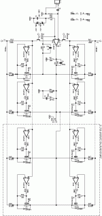
need some explanation here: HOW does this work? I mean: If you look at IC8 and IC9 (A1-2-3 and 4- where do they get their signal from? The non-nverting input is connected to the power rails??
I know this must work somehow, because velleman has been selling the kit for uite a few years now. I have tried to replicate it without the dc protection, but guess what happened :-(.
R53 started to smoke and finally burned out completely, and I have a huge dc offset on the output (+35Vdc!). I don't know how to test the drivers, because I have no experience yet with mosfets (boy are there a lot of different onces!). I didn't put a load on the amplifier...
If somebody could help me a little here?
btw: I saw on the datasheet the absolute max power supply for the TL061 is +/-18Vdc... WHY do they push this chip to the limit and put +18Vdc on the power supply pins? Can it be lowered? I measured +/-18.5Vdc on the amp... Maybe that's why the resistor blew? I haven't tested the opamp yet to see if it's alright, but I tested it in circuit and it behaves very weird, so I assume it's broken (lot's of offset and a completely distorted output on pin 6)
Attachments
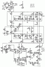
FET fraud
After a quick glance there are at least two problems, one major and one minor.
The major problem is that, as I squint to make out the schematic detail, all the FETs should be N-channel, all IRF140s. This alone will cause a meltdown.
The minor problem is that R52 appears to be a little too big. It seems the input buffer has a gain of roughly 2, and then R52 sets the main amp gain to be roughly 2 as well giving an overall gain of 4. Usually you want to have an overall gain of 20 or more. So R52 might want to be 3k3 or something.
I'd recommend that you simplify the circuit while you are trying to debug it. Like just use the A1 and A3 outputs to start with and put 10-ohm WW resistors in each line between FET and output to save the FETs if something is wrong. Then test all the dc levels and check that an ac signal can be amplified before removing the 10-ohm resistors and adding the A2/A4 sections.
The operation of this circuit is simpler than it looks. The current in the power rails of the TL071 is amplified by the A* circuits and fed to the output. The A* opamps create localised feedback to linearize the current in each FET. Feedback to the TL071 is used to control the output voltage. I think Meridien used to use (still do?) this sort of circuit.
Correction
This is what happens when one's glance is too short.
The FETs for A1 and A3 should indeed be IRF9140s (P-channel) but in the schematic the source and drain connections are shown the wrong way around. So the source should go to the V+ side and the drain to the output.
Sorry to confuse you.
BAM
This is what happens when one's glance is too short.
The FETs for A1 and A3 should indeed be IRF9140s (P-channel) but in the schematic the source and drain connections are shown the wrong way around. So the source should go to the V+ side and the drain to the output.
Sorry to confuse you.
BAM
Nah, no problem. I'm very glad you are willing to help me!
I have included the schematic as you say it should be. Looks better? I noticed that mistake indeed when I added the internal prto.diodes in the mosfets. But from what you are saying, I understand that the amplifier is actually amplifying the current drawn by the TL061P???
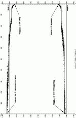
- What about the power supply? I have measured little over -18Vdc on pin 7 of IC1 (new schematic, -18.30Vdc and +17.95Vdc to be exact after 5 minutes), and that worries me because in the datasheet it says the absolute max is +/-18Vdc! Can I make a seperate power supply to feed them a safer voltage like +/-15Vdc or change the zenerdiodes ZD9 and ZD10 to 16 or 17Vdc? Take a look at the scope image I will post next. That is the voltage measured on pin 7 and 4 in the original schematic . Is that normal behaviour for zener diodes? They do get a little warm. I did also notice that in the original schematic led LD34 doesnt light up (yes it's placed correctly and the leds works perfectly 'cause I tested that)
- What is the function of T5 and T6? I assume they will 'mute' the amp when the thermal contact is closed, but I don't need that, so can I just delete the part I have marked with a dotted line?
I have included the schematic as you say it should be. Looks better? I noticed that mistake indeed when I added the internal prto.diodes in the mosfets. But from what you are saying, I understand that the amplifier is actually amplifying the current drawn by the TL061P???
- What about the power supply? I have measured little over -18Vdc on pin 7 of IC1 (new schematic, -18.30Vdc and +17.95Vdc to be exact after 5 minutes), and that worries me because in the datasheet it says the absolute max is +/-18Vdc! Can I make a seperate power supply to feed them a safer voltage like +/-15Vdc or change the zenerdiodes ZD9 and ZD10 to 16 or 17Vdc? Take a look at the scope image I will post next. That is the voltage measured on pin 7 and 4 in the original schematic . Is that normal behaviour for zener diodes? They do get a little warm. I did also notice that in the original schematic led LD34 doesnt light up (yes it's placed correctly and the leds works perfectly 'cause I tested that)
- What is the function of T5 and T6? I assume they will 'mute' the amp when the thermal contact is closed, but I don't need that, so can I just delete the part I have marked with a dotted line?
Attachments
Oh, and btw: I was stupid enough to mount everything the first time to test the board and ofcourse the irfp9140 mosfets where mounted incorrectly hence explaining the +35Vdc on the output. How can I see if they are broken or not? Is it possible only the protection diode is broken, but the mosfet is ok? Maybe somebody can give me a link to a schemtic to test fets?
question..questions.. soo many questions...
Why are there two 100uF caps placed in series at the inverting inout of IC1 (TL061) in the new schematic? I know they put them like that so they are not polarized, but what is their function? Seems odd to me to have such large caps on an input of an opamp? I have a slight feeling this has something to do with amplifiation factor? Is it to make sure DC gain is reduced to zero while AC gain is controlled with R1 and R4 in the new schematic?
Traderbam: you say I will need an overall gain of 20 or more. Why is that? Simply so I can amplify a 1.5vrms signal to 30-40Vrms? Or is there another reason? And wich resistor should I change? You suggest to change R4, but why not R1 or even R3?
Will I need to put extra diodes like an 1N4007 across the mosfets to make sure clipping won't be a problem? This amp will be used in a sub amp, so clipping will defintely occur...
"Why are there two 100uF caps placed in series at the inverting inout of IC1 (TL061) in the new schematic?"
These capacitors AC couple the potential divider formed by R52 and R59 to ground, indeed rolling off extreme low freqency response. The larger their values (50uF combined in this case), the lower the bandwidth of the amp can extend. Note that this is not necessarily a good thing - no one wants to play the warps in records!
Tim.
a) "But from what you are saying, I understand that the amplifier is actually amplifying the current drawn by the TL061P???"
Yes that is correct. Seems weird at first but is sort of cunning if you think about it. Only trouble is that this assumes the supply rail currents are linearly related to the output current, which isn't necessarily so since op-amps aren't designed with this in mind.
b) "Can I make a seperate power supply to feed them a safer voltage like +/-15Vdc or change the zenerdiodes ZD9 and ZD10 to 16 or 17Vdc?"
Yes. I don't think it matters too much what the voltages are across the TL061, within reason. To be on the safe side I'd use 16V zeners or thereabouts. Assuming you've dispensed with the elaborate protection circuitry shown at the bottom of the original schematic you can also increase the values of R71/R72 to 1.8k to reduce the heat dissipation of the zeners. This will reduce their bias from some 30mA to 10mA and may help keep them a little more thermally stable.
c) "Is that normal behaviour for zener diodes?"
It looks a little odd because there seem to be two steps in the voltage before it settles. I'm not too worried about it. It would be interesting to see V+ and V- too on the same graph.
d) "I did also notice that in the original schematic led LD34 doesnt light up "
Can't really comment. If its counterpart on the plus side lights up then it should too.
e) "What is the function of T5 and T6?"
They serve two functions. The first is to limit the maximum current through the FETs - notice they measure the voltage across the 0.22 resistors and if too high they pull the opamp inputs towards their respective rails. This function could also be achieved more simply by placing zeners across the resistors from op-amp + to the rail. The second function is to do the same thing in response to the thermal switch.
f) "How can I see if they are broken or not?"
Tricky. In my experience it is not a good idea to reuse over-stressed transistors even if they appear to work. However, if you use 10-ohm resistors in the drains for safety you can turn the circuit on and see whether they are still functioning. Note the N-channels might also have been damaged.
g) "Why are there two 100uF caps placed in series at the inverting inout of IC1?"
Trwh said it. A crude and widely used means to reduce the dc offset at the output. It *may* be possible to omit the caps - but you'll have to check the dc offset at the output remains sensible over time as the amp heats up and cools down (+/- 100mV is usualy ok for a speaker) and then you can have a flat frequency response to dc (for a truely soul shaking sub woofer experience ).
).
h) "you say I will need an overall gain of 20 or more. Why is that?"
Yes to have a reasonable voltage gain. Change R4 because of offset issue above and to minimize changes to the open loop phase response.
i) "Will I need to put extra diodes..."
I would as a sensible precaution. The speaker is inductive so whenever an abrupt change in current occurs in the FETs the speaker will cause the output voltage to whip-lash to try to maintain the current. This can occur when the current limiters trigger and sometimes when the amp is power-cycled with speaker attached. IN4007s will be fine.
These are sort of brief answers. If you would like more explanation then no problem, just ask.
BAM
Yes that is correct. Seems weird at first but is sort of cunning if you think about it. Only trouble is that this assumes the supply rail currents are linearly related to the output current, which isn't necessarily so since op-amps aren't designed with this in mind.
b) "Can I make a seperate power supply to feed them a safer voltage like +/-15Vdc or change the zenerdiodes ZD9 and ZD10 to 16 or 17Vdc?"
Yes. I don't think it matters too much what the voltages are across the TL061, within reason. To be on the safe side I'd use 16V zeners or thereabouts. Assuming you've dispensed with the elaborate protection circuitry shown at the bottom of the original schematic you can also increase the values of R71/R72 to 1.8k to reduce the heat dissipation of the zeners. This will reduce their bias from some 30mA to 10mA and may help keep them a little more thermally stable.
c) "Is that normal behaviour for zener diodes?"
It looks a little odd because there seem to be two steps in the voltage before it settles. I'm not too worried about it. It would be interesting to see V+ and V- too on the same graph.
d) "I did also notice that in the original schematic led LD34 doesnt light up "
Can't really comment. If its counterpart on the plus side lights up then it should too.
e) "What is the function of T5 and T6?"
They serve two functions. The first is to limit the maximum current through the FETs - notice they measure the voltage across the 0.22 resistors and if too high they pull the opamp inputs towards their respective rails. This function could also be achieved more simply by placing zeners across the resistors from op-amp + to the rail. The second function is to do the same thing in response to the thermal switch.
f) "How can I see if they are broken or not?"
Tricky. In my experience it is not a good idea to reuse over-stressed transistors even if they appear to work. However, if you use 10-ohm resistors in the drains for safety you can turn the circuit on and see whether they are still functioning. Note the N-channels might also have been damaged.
g) "Why are there two 100uF caps placed in series at the inverting inout of IC1?"
Trwh said it. A crude and widely used means to reduce the dc offset at the output. It *may* be possible to omit the caps - but you'll have to check the dc offset at the output remains sensible over time as the amp heats up and cools down (+/- 100mV is usualy ok for a speaker) and then you can have a flat frequency response to dc (for a truely soul shaking sub woofer experience
).h) "you say I will need an overall gain of 20 or more. Why is that?"
Yes to have a reasonable voltage gain. Change R4 because of offset issue above and to minimize changes to the open loop phase response.
i) "Will I need to put extra diodes..."
I would as a sensible precaution. The speaker is inductive so whenever an abrupt change in current occurs in the FETs the speaker will cause the output voltage to whip-lash to try to maintain the current. This can occur when the current limiters trigger and sometimes when the amp is power-cycled with speaker attached. IN4007s will be fine.
These are sort of brief answers. If you would like more explanation then no problem, just ask.
BAM
heh heh heh.. would indeed be awesome if one could make frequencies <15Hz audible ...
a) On the velleman site I see this: "This audio power amplifier meets the strictest standards for quality and robustness. Using a very special circuit the end stage is always set to CLASS A, without any unnecessary loss of power. ".
Ok, so now the next question: Class A?
If this amplifier uses a trick (amplifying the current drawn by the TK061) to work wich obviously isn't something opamps where supposed to do, how can they say this is a quality amp? I mean, I'm looking for a simple-to-build amp with a power rating of +150@4Ohm for my subs. I know this one looks to be a little overkill, but I thought the desing was simple and proven to be working right (velleman has been selling them for years now). But are there simpeler designs that use components easily obtainable in Belgium? Is it worth the trouble to continue this project, or should I take a look at another amp? I've seen leach, but it's too complicated. I've also seen chips like the TDA7293, but I'm not too fund of using them.
b) You mean R70/71 I assume? Will do that! I've also been thinking about using an LM317/337 to get those voltages.
c) I've plotted V+ and V-, and they show exactly the same behavious, so it has little to do with the zeners being unstable. I still wonder though why the power supply acts like that...
d) Thought so too... I'll have to keep my head together and do some measurements on the board... Maybe I could actually fix it ;-).
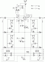
e) So to simplify things, I can ommit them (next schematic)?
f) I'm not going to take the change.. I'll put ne ones in the amp. But why would the N channels be damaged too? The IRFP140 is rated 100V across D-S...
g) Ok, got that! But you say it's a crude way of foing it. Is there a better way? You say to ommit the caps, but I assume I'll have to ground R4 (RE52 in the original schematic) on one side?
h) Can you also explain a little further what you mean by not changing the open loop phase responce? IC1 is used in a close loop here...
i) done!
new questions:
j) in the last schematic here, R11-R6 and C6 are called a boucherot network right?
k) The power resistors R32->R35 are placed between the supply lines and the mosfet. Aren't they usually placed between the mosfets and the outputs to make sure they won't fight eachother?
l) To make the system capable of driving lower impedanced like 2ohms, can I just double the driverstages like IC2B-R13-R14-T4-D2 like I did in the next schematic?
m) What about bias? How does the bias work here? I've seen most amps have a pot to control this...
n) Most amps have a resistor with a coir turned around them in series with the output. Why is that? Does that have anything to do with pop-on noise?
...a) On the velleman site I see this: "This audio power amplifier meets the strictest standards for quality and robustness. Using a very special circuit the end stage is always set to CLASS A, without any unnecessary loss of power. ".
Ok, so now the next question: Class A?
If this amplifier uses a trick (amplifying the current drawn by the TK061) to work wich obviously isn't something opamps where supposed to do, how can they say this is a quality amp? I mean, I'm looking for a simple-to-build amp with a power rating of +150@4Ohm for my subs. I know this one looks to be a little overkill, but I thought the desing was simple and proven to be working right (velleman has been selling them for years now). But are there simpeler designs that use components easily obtainable in Belgium? Is it worth the trouble to continue this project, or should I take a look at another amp? I've seen leach, but it's too complicated. I've also seen chips like the TDA7293, but I'm not too fund of using them.
b) You mean R70/71 I assume? Will do that! I've also been thinking about using an LM317/337 to get those voltages.
c) I've plotted V+ and V-, and they show exactly the same behavious, so it has little to do with the zeners being unstable. I still wonder though why the power supply acts like that...
d) Thought so too... I'll have to keep my head together and do some measurements on the board... Maybe I could actually fix it ;-).
e) So to simplify things, I can ommit them (next schematic)?
f) I'm not going to take the change.. I'll put ne ones in the amp. But why would the N channels be damaged too? The IRFP140 is rated 100V across D-S...
g) Ok, got that! But you say it's a crude way of foing it. Is there a better way? You say to ommit the caps, but I assume I'll have to ground R4 (RE52 in the original schematic) on one side?
h) Can you also explain a little further what you mean by not changing the open loop phase responce? IC1 is used in a close loop here...
i) done!
new questions:
j) in the last schematic here, R11-R6 and C6 are called a boucherot network right?
k) The power resistors R32->R35 are placed between the supply lines and the mosfet. Aren't they usually placed between the mosfets and the outputs to make sure they won't fight eachother?
l) To make the system capable of driving lower impedanced like 2ohms, can I just double the driverstages like IC2B-R13-R14-T4-D2 like I did in the next schematic?
m) What about bias? How does the bias work here? I've seen most amps have a pot to control this...
n) Most amps have a resistor with a coir turned around them in series with the output. Why is that? Does that have anything to do with pop-on noise?
Attachments
Peter,
"n) Most amps have a resistor with a coir turned around them in series with the output. Why is that? Does that have anything to do with pop-on noise?"
No, the coil forms an inductor which helps prevent the amp from oscillating when driving capacitative loads, like long speaker leads.
This amp design was said to be prone to oscillation here:
http://www.diyaudio.com/forums/showthread.php?s=&threadid=1283
If you are intent on using this design, an output inductor is the sort of addition to the circuit that could help make it more stable. Please post your experiences / comments regarding this design if you go ahead!
Hope this helps,
Tim.
Peter,
In response to your points:
a) I imagine all companies say they meet the strictest standards etc. Using an op-amp like this can be fine, don't get me wrong.
e) You can omit the protection, as long as you don't mind being unprotected.If you accidentally short circuit the outputs...say when changing speaker cables or whatever you may blow the output transistors.
f) Sometimes when one set of output transistors blow they short circuit and the opposing transistors see a short and then exceed their maximum current and blow as well. Worth checking all your transistors are ok.
g) Yes, you would have to ground the C1 end of R4.
h) To increase the closed-loop gain you can either decrease R4 or increase R1. It is not easy to determine the affects on the phase margin of the circuit without simulating it or building it. Without this knowledge I advise reducing the value of R4. It may be necessary to change the value of C4 as well. If you tell me what closed loop gain you want I'll do some maths and come up with a proposal for R4 and C4 values. C4 provides what is called phase-lead compensation and affects the phase margin of the design.
j) "boucherot"? Je ne sais pas!
k) These resistors follow the source pin. They are used for balancing current flows when FETs are used in parallel - like connecting all the pins of one device to those of the next (more or less) except for the source pins which are then connected by these balancing resistors. In this design they are not really being used for this, rather as current sensors for the opamp drivers.
l) You can make the amp capable of more power output in several ways. You can use meatier devices than 140s or you can improve heatsinking or you can add more output stages. The latter can be done easily but each time you add a stage the transconductance of the amp is increased and this will affect its phase margin. Some adjustments would have to be made to restore the stability - eg reducing the value of R2 and adjusting C5. I'd concentrate on getting it working as it stands for the moment.
m) It looks like the bias is set by the steady-state supply current of the TL061. This sets a dc voltage across R12 and R22 and the output opamps make the voltages across R32-R35 the same. The TL061 bias current is fixed internally and is temperature compensated (this is possible in opamps because all the transistors share the same wafer).
n) See Tim's answer. Nothing to do with switch-on noise. An output inductor helps prevent a capacitive speaker or speaker cable from reducing the phase margin of the amplifier too much. To put it simplistically, amps tend to oscillate when you put a capacitor across their outputs. An inductor is like an anti-capacitor and helps mitigate this problem. To explain this properly will require a lot of text!
There are much simpler circuits around that will meet your needs just as well as the Velleman. By the way, just what are your needs - 200W into 4 ohms for a subwoofer? I think the Velleman is fine too. Unfortunately I don't have any schematic drawing tools just now so perhaps someone else will post an alternative, simpler circuit or a link to one (thanks).
Well, I've been thinking about this amp. I know all components are easely obtainable here in Belgium, it's not very expensive, I now understand a lot more of the schematic and to be honest: I dopn't know why, but the desing appeals to me.
I'll try to make it again (already blew up my first try 'cause those drivers where mounted incorrectly in the original schemtic.
h) Thanks for the offer, but I don't want to be such a burdon. I'll siply try to make the amp the way it says in the original schematic, except for some errors I'll have to fix (like the drivers)
n) I got the picture! i'll add the coil and resistor just to be sure... I take a 10W-1Ohm res. with some copper wire around it will do? I don't suppose it's that critical...
Thanks for you enormous help! I really appreciate it. When I blew up the first amp I just wanted to throw it away and use another design. Now, I'm feeling eager to get this one up and running. When it's done, I'll post my findings!
Thanks guys for your help!!
Peter
Banned
Joined 2002
Hi
"I take a 10W-1Ohm res. with some copper wire around it will do?"
Most people use a 3W 10 Ohm resistor. The resistor prevents the coil from ringing at high frequencies, I think a large value is a better bet.
Good luck with the project - like I say please do post pics / comments!
Tim.
"I take a 10W-1Ohm res. with some copper wire around it will do?"
Most people use a 3W 10 Ohm resistor. The resistor prevents the coil from ringing at high frequencies, I think a large value is a better bet.
Good luck with the project - like I say please do post pics / comments!
Tim.
- Status
- This old topic is closed. If you want to reopen this topic, contact a moderator using the "Report Post" button.
- Home
- Amplifiers
- Solid State
- Velleman K4020 schematic