hi,
Before I'll make my first own pcb, I'd like you to check my layout for mistakes or obvious improvements.
The circuit is an electret microphone preamp. In my current version, it works well with through-hole components and standard audio op-amps, but some higher speed op-amps that have a promising noise/quiescent current ratio didn't work.
Now I thought I'd make a star ground on my pcb, hoping that eg. the LT6234 will work on it. (Also, I'd like to make the whole thing even more compact, well..., and nicer to look at)
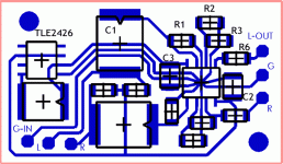
The schematic only includes one channel, and it misses the resistor to feed the mic, which is on the pcb, near C1, of course.
link to the schematic
Thanks for looking!
Dominique
Before I'll make my first own pcb, I'd like you to check my layout for mistakes or obvious improvements.
The circuit is an electret microphone preamp. In my current version, it works well with through-hole components and standard audio op-amps, but some higher speed op-amps that have a promising noise/quiescent current ratio didn't work.
Now I thought I'd make a star ground on my pcb, hoping that eg. the LT6234 will work on it. (Also, I'd like to make the whole thing even more compact, well..., and nicer to look at)
The schematic only includes one channel, and it misses the resistor to feed the mic, which is on the pcb, near C1, of course.
link to the schematic
Thanks for looking!
Dominique
Attachments
Hi,
what are the two large components, one below TLE and the other below C1?
The decoupling caps (C1 & C2) should be returned to a power (dirty) ground not shared with the signal ground. They should also be VERY close to the opamp pins and should have the very shortest lead lengths to help prevent voltage spikes getting back to the grounds. You could also add a cap direct across the power pins of the opamp (10nF ceramic) underneath the opamp to minimise the lead lengths.
Where are your power input connections?
Oh, I forgot to mention that I'll put a battery on the other side of the pcb and afterwards, I'll look where I can make the connection to the circuit side
The one below the TLE2426 rail splitter is the 1uF noise reduction cap like recommended in the datasheet, the other one is a DC blocking cap (just like C1, but for the other stereo channel).
I tried to follow the recommendations and make a star ground, so I returned all the grounds to one single point, but I think I understand your recommendation. I'll think on how to realize it on my pcb.
The decoupling caps, C2 and C3 are already very near to the op-amp pins, aren't they?
Thanks for your hints,
Dominique
AndrewT said:Hi,
what are the two large components, one below TLE and the other below C1?
The one below the TLE2426 rail splitter is the 1uF noise reduction cap like recommended in the datasheet, the other one is a DC blocking cap (just like C1, but for the other stereo channel).
The decoupling caps (C1 & C2) should be returned to a power (dirty) ground not shared with the signal ground. They should also be VERY close to the opamp pins and should have the very shortest lead lengths to help prevent voltage spikes getting back to the grounds. You could also add a cap direct across the power pins of the opamp (10nF ceramic) underneath the opamp to minimise the lead lengths.
I tried to follow the recommendations and make a star ground, so I returned all the grounds to one single point, but I think I understand your recommendation. I'll think on how to realize it on my pcb.
The decoupling caps, C2 and C3 are already very near to the op-amp pins, aren't they?
Thanks for your hints,
Dominique
Hi,
my mistake, I did not recognise the soic with the star ground underneath it. Will you be able to solder the soic on top side without an accidental short from pin to ground?
C2 & C3 are located OK.
To preserve the layout, how about a jumper from C3 common to C2 common then track to Pground adjacent to Sground? Not as neat as your's but functional and short. Alternatively 2 layer PCB.
But having done this well I'm sure you'll find a neater solution.
AndrewT said:Hi,
my mistake, I did not recognise the soic with the star ground underneath it. Will you be able to solder the soic on top side without an accidental short from pin to ground?
I hope so!
") I read articles on how others do SMD work and I simply want to try.
I read articles on how others do SMD work and I simply want to try.
C2 & C3 are located OK.
To preserve the layout, how about a jumper from C3 common to C2 common then track to Pground adjacent to Sground? Not as neat as your's but functional and short. Alternatively 2 layer PCB.
But having done this well I'm sure you'll find a neater solution.
Ok, I think I'll have to investigate on where I connect the battery, because right now, I'm still missing that Power ground (that's what you mean by pground, do you?)
Would a two sided pcb with a ground plane be a better solution to make more op-amps work fine in that circuit?
Cheers,
Dominique
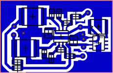
In the meantime I tried to read some more texts about pcb layout and decided to make an attempt with a groundplane on the same layer as the signal traces.
The high current grounds... that of the op-amp power supply pin's decoupling caps, the power-supply ground and the signal-out-return are now very near and the trace is widened. The grounds having to handle lower signal currents are a bit farther away.
That groundplane isn't very nice looking by now, but please could anyone tell me if that approach is ok, or if there's something terribly wrong with my layout?
It's still the same circuit, not much more than a simple non-inverting op-amp circuit using a dual op-amp. But now the TLE2436 is on the other side to get the high currents closer together.
I hope the pcb material will arrive in a few days and I can't wait to make that first pcb of mine - I just don't want it to be a mess!
Best wishes,
Dominique
Attachments
- Status
- This old topic is closed. If you want to reopen this topic, contact a moderator using the "Report Post" button.