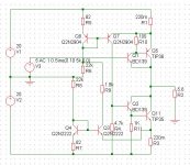
Having defined the requirements for my ideal output stage, e.g. a push pull output in which the two halves maintain a reasonable quiescent current and the hand over is a gentle curve rather than abrupt switching. I came up with the circuit shown below. I’m sure this has been done before, so I thought I'd post this circuit for comment.
The basic concept is a single sided amp, in this case a CEF, with an active load.
The load tries to maintain the quiescent current of say 300mA in the main transistor.
Note: The devices and values were just those I used to see if it worked as intended, and get some idea of stability from spice simulations. So I've know idea how well this would work in the real world.
Attachments
hm...
you intend to run it in class A?
Am I right that you suggested it provides sweeping bias? If so, how?
It looks interesting but I probably don't understand it in details...
Did you consider high frequency phase shift? It may be significant with these current sensors and feedbacks and in end lead to cross conduction at HF.
Could you add some more comments about how it works?
regards
Hi darkfenriz,
yes the intention is class A operation, and I’m not sure I call it sweeping bias I tend to think of it as an active load.
I just thought it was an interesting idea, and after playing around with simulations I think the basic circuit can be made to work.
So I thought I’d put it up for comments, and see if anyone had similar or alternative ideas.
Any way an explanation of how I intended it to work is as follows:
Q1 & Q5 are a simple CEF that provide the main signal amplifier, which is maintained in class A operation by everything else.
The current sensor Q7 senses the current in Q5 via R1 and if it
goes below the threshold set by Q8 the error signal turns on the
darlington Q2 & Q11, which restores the quiescent current to
Q1 & Q5.
Obviously with a simple resistive this is the condition for the
negative half cycle when Q1 & Q5 would normally be heading
for cut off. And since there is no direct drive to Q2 & Q11 it’s the
amplified error signal that supplies the load and the quiescent
current for Q1 & Q5.
When in the positive half of the cycle, the current through
Q1 & Q5 is high enough to turn off the sense device Q7,
so the darlington Q2 & Q11 would also be turned off.
To prevent this a second current sense device Q3 with threshold
set by Q4, senses the turn off of Q2 & Q11 and sends the error
signal to Q8, which alters the threshold for Q7 thus turning it on
and restoring the conduction of Q2 & Q11.
So the main output devices never turn off, and only the small
signal sensor transistor Q3 is ever reverse biased. And I expect
it can recover quickly enough from this state not to cause problems.
I have also played with the idea of removing Q3 & Q4 and
replacing them with a simple diode string that maintains a
nominal bias on Q2 & Q11, but the change over trends to be
a bit abrupt.
As for HF stability, with so many feed back paths I expect that
could be a problem, although in simulation this hasn’t shown up
as a serious issue. But then I’m not sure how far I trust the
simulation in this respect.
Cross conduction is a problem with the devices shown, as they
are slow and the delays in the active load Q2 & Q11 cause
higher quiescent current at high frequencies. In this case
a 10volt signal at 25kHz is starting to increase the quiescent current. Simulating with faster devices such as 2SA1302 & 2SC3281 suggests that this problem can be moved to a higher
frequency, but greater care is required in the choice of drivers, as HF stability becomes more of a problem.

- Status
- This old topic is closed. If you want to reopen this topic, contact a moderator using the "Report Post" button.