sam9 said:As point of clarity do you mean "emitter resistors" or "Collector resistors"?
Collector resistors. To isolate the transistors from the speaker output.
EWorkshop1708 said:Instead of having a base resistor for each power device, couldn't I just have one base resistor that feeds the base leads of the power transistors since they are connected together?
This should work - it's primarily to isolate the transistors from the speaker load. Be aware that for a CFP, the emitters of the drivers must connect directly to the output's collectors, not after the collector resistor.
EWorkshop1708 said:Also, since the collectors are all connected, instead of using several "emitter" resistors to each collector of the outputs, couldn't I just use one for each set of 5 transistors?
No. The idea is to reduce the interaction between devices that would cause parasitic oscillation. They should be as close to the base terminal of the output devices as possible.
You may also want to try the old resistor-with-inductor-wound-on-it to isolate out the capacitance of the speaker cable. Many say this is unneccesary these days, though.
sam9 said:As point of clarity do you mean "emitter resistors" or "Collector resistors"? The output is taken off the collectors and he already has emitter resistors (0.13R).
A CFP pair essentially behaves like the first transistor in the pair (the 'driver'). Therefore:
If one driver drives several power transistors in a CFP, all the power transistors need emitter resistors for proper current sharing. The original diagram shows these., but as far as the CFP as a whole is concerned regarding thermal stability they are largely 'invisible'.
In order to get the Vbe multiplier to track thermally, you may need \emitter' resistors for the whole CFP, i.e. the driver E connection with power transistor C's is the CFP's 'emitter' and you insert a small value resistor from here to the output of the amp, as you would if it was an EF configuration.
These will be on the order of all the emitter resistors of the power transistors, in parallel, and sometimes even smaller - see a thread here regarding bias current adjustment for CFPs - in general, in parallel output transistor EF stages, you need a 'per pair' bias current, which can add pretty quickly. CFPs behave slightly differently and usually require less bias current, so for all it's trickyness, the CFP has an efficiency advantage when paralleling output transistors.
EWorkshop1708 said:Instead of having a base resistor for each power device, couldn't I just have one base resistor that feeds the base leads of the power transistors since they are connected together?
In theory, yes, but in practice, you may run into trouble, especially if your driver is on the PCB and your outputs on an outboard heatsink. The idea is to damp the resonant circuits frmed from the transistor capacitance and various lead inductances. Since power transistors tend to be large and you need to spread them out on the heatsink, wire lengths become a problem. Adding a base series resistor for each of the power outputs would be the sure-fire way, besides, normally it gives you a 'free jumper' on the PCB and makes routing easyer.
Also, since the collectors are all connected, instead of using several "emitter" resistors to each collector of the outputs, couldn't I just use one for each set of 5 transistors?
As I explained above, yes - in fact this is the proper way to do it as all the collectors AND the emitter of the driver are the CFPs 'emitter', so you add an emitter resistor for the whole CFP. I have seen it done in other ways, for instance only the first output pair has the resistor, the others connect directly to the output rail. This configuration effectively makes the output a current mirror configuration, where for n power transistors, power transistor 2 to n mirror the current in power transistor 1. The particular configuration also used higher value emitter resistors for the power transistors, 0.22 ohm IIRC, and all power transistors need to be in thermal contact (i.e. common heatsink) - but it was not intended for audio.
What are the diodes for, to keep the input drive voltage from exceeding the rails?
They work with the proposed VAS emitter resistor to limit the maximum source current of the VAS, by limiting maximum input voltage.
regarding 100 ohm resistors for the Diff stage, I thought that the purpose of using resistors in the diff stage was to reduce offset.
They do reduce offset as a consequence of lowering total LTP gm, because that way the differences are lower too. But this is not their primary function - they linearize the input stage, and the reduction in gain can be made up for by higher tail current (but at the expense of higher bias and oftenm noise current, which can be a non-issue if the amp is driven from a low impedance source). If you are after offset reduction, a current mirror terminationof the LTP will be of great help there.
BTW your offset adjustment also adjusts the open loop gain of the amp to an extent, and, you can adjust the offset with a WAY to large range - practically from + to - rail voltage. One slip of the screwdriver...
It's really not a good idea to save on parts for the front end - extras like a fed diodes and resistors, and even transistors, are likely to cost less thana single power transistor...
Good news, I got the amplifier to stop oscillating!
I'll post an updated schematic shortly, but I wanted to update the thread.
I added extra low uf caps on the power rails, and also some small caps on the drivers to tame the output stage.
Also added several resistors in different places, and now I have 0.15 Ohm output resistors instead of none like before.
Also changed the Bias POT and also the Offset POT to lower values
I'll have to do some testing with higher voltage, but with my pair of 9V batteries, the amp was real quiet at full volume with no signal, sounded good with bass and treble. Had about 3-8mV offset at the most after adjusting one time. So far, the CFP output stage seems to be a winner, but I'll see how it plays once I get a transformer to get some real power out of this thing.
BTW, I'm wanting to have rails that avg around +/- 55 or 60V loaded, with a 4ohm load, 300-400W RMS, what transformer would you recommend?
I was looking at a 50-0-50 625VA trans, but I'm wondering if that would be too much.
Your instability problem arises from a too slow turn off of the output devices.
B-E junctions of the ouput devices are charged very quickly through the non-emitter-degraded drivers but slowly discharged through the 56 ohm bleeder resistors.
Try something below 10 ohms, maybe 5.6 ohms, this will make a huge stability improvement at the expense of higher driver dissipation.
That's one of the main flaws of CFP output stages.
Adding a 100nF capacitor between the upper bases and lower bases of the output devices may also help. This was suggested by somebody some time ago, altough I've tried it without success.
Anyway, after looking at rail current waveforms with an oscilloscope and seeing how much parasitistic cross-conduction is generated (particularly with trebble signals), I no longer wanted to use CFP.
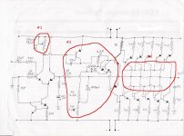
Strange circuit. 
I see a couple of problems here.
#1) Lose that rheostat. That is not the way to adjust for DC offset in a LTP. Use a much smaller pot, 500 ohms, and connect the ends to each emitter of the diff pair. The CCS connects to the center terminal (the moving element). This allows for compensation for DC offset, and adds a bit of emitter degeneration that will improve the performance of the LTP.
#2) Select either a bootstrapped VAS or use a CCS: one or the other, but not both. That bias adjustment is also crazy. See This Schematic of a solid state amp I designed. Pay close attention to how I arranged for bias adjustment in the VAS stage (Q6 and Q7) and how the drivers for the finals are connected to it. This bias method compensates for overheating of the finals. Which brings us to another problem, already mentioned.
#3) You need resistors between the collectors and the output. These need be but small valued resistors. Again refer to my design: these are current sense resistors that provide the "feedback" information that the bias compensation network needs to "know" so far as how the finals are working. As the finals heat up and attempt to draw more current, the voltage drop tries to rise, and the bias current is reduced accordingly. Now, you won't be needing such large resistors, since your design is more powerful. Since you already have 0.13 ohm resistors, simply move them from the emitters to the collectors.
I'm not so certain that the problem is oscillation, as that it may very well be that your bias network can't stably set a larger Q point current without losing control.
Attachments
Thanks for all of your replies!!!
Now I've finally got the chance to draw a new schematic after doing several modifications to the original design.
The bias adjusts really good, I tried anywhere between 6-1000mA just playing around, and it adjusts well, and the bias current doesn't fall or rise very much once set. I also changed a few existing part values besides adding other new parts.
So far the amp behaves well, and sounds very clean full range (even though it's gonna be used for bass)
I like the sound of the On-Semi transistors.
This amp sounds very good once I get the bias over 50-60mA. I can't wait to try more power and see if the amp behaves just as well.
Any more suggestions, feel free to comment.
Attachments
Hi EW,
Do you mean 50-60mA per device or for the output stage collectively as measured across the 0.15R resistors to output?
More suggestions -
Do you really need those 1nF on the CFP BC's ?
And why not try some emitter degeneration for the input pair and reduce the Vas 100pF correspondingly for lower HF distortion and wider BW.
A handy pair of 2SK170's and you could see if you prefer FET input - drop in, listen.
Cheers,
Greg
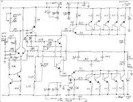
To clarify a few things about the schematic:
The 23,500 uf caps are really 5 parallel 4,700 uf caps, but I didn't have enough room to draw a row of them, so I just drew one.
For HF filtering:
Used 1KV 10nf (103 on the cap) filter caps from PSU input of computer supply to filter the incoming DC for the power side, followed by ceramic 250V 0.27uf caps close to the transistors and GND.
To stabilize the output:
I added 100 ohm driver base resistors, and 4.7 ohm emitter resistors, and 1nf caps between B-C of the drivers. Added 1 ohm in series with base lead wire of the outputs. Also now have 0.15 ohm output resistors. Also have an output inductor and two-stage Zobel.
PCB with input stages:
Dedicated 80V 4,700 uf power filter caps
2KV 2.2nf caps to bypass HF signals.
Small toroids filter incoming DC
Added 47 ohm resistor to emitter of VAS.
Changed POTS to 680 for offset connected to 100 ohm resistor, and 4.7K for bias adj. Added 47 uf cap and 470pf caps for Bias adjust.
amplifierguru said:Hi EW,
Do you mean 50-60mA per device or for the output stage collectively as measured across the 0.15R resistors to output?
No, 50-60 mA total. I'm using an ammeter in series with power leads, and also measured the 0.15 output resistors.
Do you really need those 1nF on the CFP BC's ?
I figured I'd try the miller effect to see if it would give me some stability. I figured also the 100ohm resistors along with the 1nf caps teamed together would bypass high frequencies from the input leads of the output stage drivers.
And why not try some emitter degeneration for the input pair and reduce the Vas 100pF correspondingly for lower HF distortion and wider BW.
A handy pair of 2SK170's and you could see if you prefer FET input - drop in, listen.
I'm not really concerned with the HF performance because it will be driving a sub, but I may try FET if I build another amp. I haven't messed with FET much, but have been curious. But actually the HF sounds really good, even though I'm not shooting for treble performance.
Thanks all you folks here at diyAudio!
Because of the several replies, and helpful tips from you folks the BIAS now adjusts properly, and the amp doesn't oscillate. Also the amp sounds different than when it was first built, there's more bass, and the amp makes almost no hiss and doesn't make hum noise anymore when putting a screwdriver near the PCB or any other hum unless you touch the input with your fingers while not touching GND at the same time.
Also there's a copper strip that runs along the edge around the perimeter of the underside of the PCB, and I connected that to GND.
Thanks once again, when I do further work on this amplifier, I'll start a new thread. I'm currently looking for a transformer preferably Toroid, in the range of 45-50V or so, that can handle driving a 4 ohm load well without dropping too much volts. My filter caps are only 80V so I don't want the peak voltage much past +/- 70-75V, but I'd be happy if it can provide 55-60V RMS at full load
If you still have suggestions or tips, please post. I appreciate all of your replies!
- Status
- This old topic is closed. If you want to reopen this topic, contact a moderator using the "Report Post" button.
- Home
- Amplifiers
- Solid State
- Strange biasing issue when adjusting VBE