Is there any limitation in the lowest possible/practical value
for the emitter resistor of a push-pull BJT output stage? I want
to parallel multiple 2SA1943/2SC5200 transistors. My simulation
shows that decreasing the value of the emitter resistor value
significally reduces the distortion generated in a triple EF. This
is because gm is higher, more linear and also spread over a wider
voltage band which redueces crossover distortion in a class AB
output stage. Because real transistors are not equal they have
to be selected. My transistors used (all the same datecode and bought
from Arrow) are selected to about 2mV Ube. Out of a lot of 25 I
have differencies in Vbc of nearly 40mV.
Currently I'm ended with a value of 0.12ohm, with about 70ma for
each transistor. This results in a voltage drop of about 9mV across
the emitter resistors. When mounting these multiple transistor bank
to a heatsink (0.5 K/W) in two banks of 3 at the upper and 3 the lower
side of the heatsink, I expect a thermal difference between these
two banks from maybe 5K (not measured yet). This would result in a
current difference between this two banks of about 30%.
The question is: May the value of the resistors lowered further
or will this result in thermal instability? (I have some amps seen
blown by this effect!)
bocka said:Is there any limitation in the lowest possible/practical value
for the emitter resistor of a push-pull BJT output stage?
In general not less than 0R1, and no greater than 0R22.
Lowering the value of the output emitter resistors much more may get you into layout effects; the individual traces' inherant resistance may start to become significant.
MOSFETs without the equivalent emitter resistors aren't
uncommon, but I'll bet you'll need at least .1 ohm to help
make a bipolar design reasonably bullet-proof.
Carefully matching gain and thermal conditions would
possibly help. How many transistors can you afford to
blow up testing your hypothesis?")
How much lower is distortion in your simulation with lower
emitter values? I'm using .27 ohm in my Leach amp simply
because I had a supply of those parts, but I also have .22
and .1. I wanted to try banks of four and five pairs with
higher rail voltages, but my supply of output transistors is
very limited, and so is my budget!
MOSFETs without the equivalent emitter resistors aren't
uncommon, but I'll bet you'll need at least .1 ohm to help
make a bipolar design reasonably bullet-proof.
Carefully matching gain and thermal conditions would
possibly help. How many transistors can you afford to
blow up testing your hypothesis?
How much lower is distortion in your simulation with lower
emitter values? I'm using .27 ohm in my Leach amp simply
because I had a supply of those parts, but I also have .22
and .1. I wanted to try banks of four and five pairs with
higher rail voltages, but my supply of output transistors is
very limited, and so is my budget!
In general you should have 12-22mV across each emitter resistor. Going too low will cause problems, not only in thermal instability, BUT with the transistion between class A and class AB. Going too high will also cause added distortion in the transition between class A and class AB.
Rather than simularing different values, I tried it once some time ago. 0.1R is a stated above the lowest. (Actually it is hard to find ordinary sandcast resistors below this value.) However, using a themocouple to measure how hot the ouput devices became I concluded that 0.1R was too small to dependably prevent "current hogging". Sometimes it is Ok and sometimes not. Closely matching output transistors may well make the lower value sufficient.
On the other hand 0.22R never showed any sign of "current hogging" (as reflected by temperature). BTW, I used the temperatur of the output devices as as indicator because the DMM I had at the time wasn't real accurate with low R values and voltages the calculated current was a little ambiguous.
In addition to lower distortion using the lowest RE values you get a small bonus of a couple more watts!
john curl said:In general you should have 12-22mV across each emitter resistor.............
This is misleading, as it is as dependant on the value of quiescent current as the size of the resistors themselves.
Use a heat gun
Build it up, debug it, then do this test:
Hit one output device with a heatgun, and monitor it's current. The resistor needs to be large enough to prevent thermal runaway. Don't let the amp sit powered up without supervision until you're sure it won't go into thermal runaway.
Build it up, debug it, then do this test:
Hit one output device with a heatgun, and monitor it's current. The resistor needs to be large enough to prevent thermal runaway. Don't let the amp sit powered up without supervision until you're sure it won't go into thermal runaway.
Hi John Thanks for input on this tyopic i asume that the 12-20Mv be the target voltage and select your actuial resistor value to obtain a 12-20 mV reading across each emitter resistor at your operating current and so the actual resistor values should be selected to acomidate these conditions is this correct?
Thanks for all your replies!
I started this thred after reading and validating Mr. Leachs article "Can Transconductance Doubling occur in Class-AB output stages?" Well, first I simulated this behavior with the spice netlist in this article (and solved the error in the fig. 9 netlist). Because this netlist uses only theoretical bjt values next I changed to the MJL3281/MJL1303 BJT output models and made a practicle EF i.e. a EF with typical values for the emitter resistors.
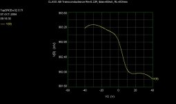
Simulating this I can see that reducing the emitter resistors to values below 0.3 ohms have a positive effect to the distortion distribution because higher orders are reduced. Paralleling BJTs have also a positive influence to minimise distortion.
When I looked to the transconductance of this stage it its far away from the thoretical curve that is used to explain transconductance doubling.
The netlist used:
CLASS AB Transconductance Re=0.22R, Ibias=60mA, RL=8Ohms
VS 1 0 DC 0
VPLUS 4 0 50
VMINUS 5 0 -50
VB1A 2 1 1.17
VB2A 1 3 1.17
Q13 4 2 12 Q2SC4793
Q14 5 3 13 Q2SA1837
R1 12 13 9.4
Q1 4 12 16 Qmjl3281a
Q2 5 13 17 Qmjl1302a
RE1 16 8 0.22
RE2 17 8 0.22
Q3 4 12 18 Qmjl3281a
Q4 5 13 19 Qmjl1302a
RE3 18 8 0.22
RE4 19 8 0.22
Q5 4 12 20 Qmjl3281a
Q6 5 13 21 Qmjl1302a
RE5 20 8 0.22
RE6 21 8 0.22
Q7 4 12 22 Qmjl3281a
Q8 5 13 23 Qmjl1302a
RE7 22 8 0.22
RE8 23 8 0.22
Q9 4 12 24 Qmjl3281a
Q10 5 13 25 Qmjl1302a
RE9 24 8 0.22
RE10 25 8 0.22
Q11 4 12 26 Qmjl3281a
Q12 5 13 27 Qmjl1302a
RE11 26 8 0.22
RE12 27 8 0.22
RLA 8 0 8
Etransconductance 9 0 VALUE = { (V(8) + 4.136E-03) / V(1) }
Ra 9 0 1e6
.MODEL Qmjl3281a npn
+IS=6.5498e-11 BF=139.247 NF=1.00176 VAF=46.776
+IKF=10 ISE=7.75232e-12 NE=3.34341 BR=4.98985
+NR=1.09511 VAR=4.32026 IKR=4.37516 ISC=3.25e-13
+NC=3.96875 RB=11.988 IRB=0.111742 RBM=0.102914
+RE=0.00127227 RC=0.209833 XTB=0.115253 XTI=1.03146
+EG=1.11986 CJE=1e-07 VJE=0.4 MJE=0.450375
+TF=7.04629e-10 XTF=1000 VTF=2.06045 ITF=41.8156
+CJC=5e-10 VJC=0.4 MJC=0.85 XCJC=0.959922
+FC=0.1 CJS=0 VJS=0.75 MJS=0.5
+TR=1e-07 PTF=0 KF=0 AF=1
.MODEL Qmjl1302a pnp
+IS=8.89983e-13 BF=72.008 NF=0.851386 VAF=10
+IKF=3.536 ISE=2.74887e-13 NE=1.03936 BR=3.08009
+NR=0.819265 VAR=96.5345 IKR=5.30959 ISC=9.64802e-16
+NC=2.56932 RB=0.931071 IRB=0.265332 RBM=0.931071
+RE=0.0001 RC=0.0345218 XTB=1.00517 XTI=1
+EG=1.05 CJE=1e-07 VJE=0.894923 MJE=0.85
+TF=3.99292e-10 XTF=1000 VTF=750.611 ITF=97.2457
+CJC=5e-10 VJC=0.95 MJC=0.23 XCJC=0.845701
+FC=0.8 CJS=0 VJS=0.75 MJS=0.5
+TR=1e-07 PTF=0 KF=0 AF=1
.MODEL Q2SA1837 PNP
+ IS=1.7671E-12
+ BF=160.54
+ VAF=500
+ IKF=1.7316
+ ISE=38.620E-12
+ NE=1.7292
+ BR=3.9832
+ VAR=100
+ IKR=1.6615
+ ISC=108.00E-12
+ NC=1.4213
+ RB=1.0611
+ RC=.23351
+ CJE=2.0000E-12
+ CJC=72.874E-12
+ MJC=.33333
+ TF=1.6596E-9
+ XTF=.61407
+ VTF=36.102
+ ITF=.70845
+ TR=10.000E-9
.MODEL Q2SC4793 NPN
+ IS=1.8747E-12
+ BF=109.30
+ VAF=500
+ IKF=4.9998
+ ISE=4.0382E-12
+ NE=1.5341
+ BR=.35724
+ VAR=100
+ IKR=1.1273
+ ISC=14.741E-12
+ NC=2.2201
+ RB=1.5379
+ RC=.19892
+ CJE=2.0000E-12
+ CJC=48.582E-12
+ MJC=.33333
+ TF=1.7700E-9
+ XTF=.61
+ VTF=30
+ ITF=.7
+ TR=10.000E-9
.DC VS -40.05 40 0.1
.OPTION NUMDGT=7
.PRINT DC V(9)
.END
Also this is a Class-AB stage I cannot see something like crossover distortion. Making a distortion analysis with a Triple-EF and added VAS driver stage shows, that lowering the emitter resistors further to 0.12 ohms, I get a significant reduction in higher order components. On the other side I know very good by practical experience that thermal runaway is a very strange problem sometimes it takes days when it occurs.
I started this thred after reading and validating Mr. Leachs article "Can Transconductance Doubling occur in Class-AB output stages?" Well, first I simulated this behavior with the spice netlist in this article (and solved the error in the fig. 9 netlist). Because this netlist uses only theoretical bjt values next I changed to the MJL3281/MJL1303 BJT output models and made a practicle EF i.e. a EF with typical values for the emitter resistors.
Simulating this I can see that reducing the emitter resistors to values below 0.3 ohms have a positive effect to the distortion distribution because higher orders are reduced. Paralleling BJTs have also a positive influence to minimise distortion.
When I looked to the transconductance of this stage it its far away from the thoretical curve that is used to explain transconductance doubling.
The netlist used:
CLASS AB Transconductance Re=0.22R, Ibias=60mA, RL=8Ohms
VS 1 0 DC 0
VPLUS 4 0 50
VMINUS 5 0 -50
VB1A 2 1 1.17
VB2A 1 3 1.17
Q13 4 2 12 Q2SC4793
Q14 5 3 13 Q2SA1837
R1 12 13 9.4
Q1 4 12 16 Qmjl3281a
Q2 5 13 17 Qmjl1302a
RE1 16 8 0.22
RE2 17 8 0.22
Q3 4 12 18 Qmjl3281a
Q4 5 13 19 Qmjl1302a
RE3 18 8 0.22
RE4 19 8 0.22
Q5 4 12 20 Qmjl3281a
Q6 5 13 21 Qmjl1302a
RE5 20 8 0.22
RE6 21 8 0.22
Q7 4 12 22 Qmjl3281a
Q8 5 13 23 Qmjl1302a
RE7 22 8 0.22
RE8 23 8 0.22
Q9 4 12 24 Qmjl3281a
Q10 5 13 25 Qmjl1302a
RE9 24 8 0.22
RE10 25 8 0.22
Q11 4 12 26 Qmjl3281a
Q12 5 13 27 Qmjl1302a
RE11 26 8 0.22
RE12 27 8 0.22
RLA 8 0 8
Etransconductance 9 0 VALUE = { (V(8) + 4.136E-03) / V(1) }
Ra 9 0 1e6
.MODEL Qmjl3281a npn
+IS=6.5498e-11 BF=139.247 NF=1.00176 VAF=46.776
+IKF=10 ISE=7.75232e-12 NE=3.34341 BR=4.98985
+NR=1.09511 VAR=4.32026 IKR=4.37516 ISC=3.25e-13
+NC=3.96875 RB=11.988 IRB=0.111742 RBM=0.102914
+RE=0.00127227 RC=0.209833 XTB=0.115253 XTI=1.03146
+EG=1.11986 CJE=1e-07 VJE=0.4 MJE=0.450375
+TF=7.04629e-10 XTF=1000 VTF=2.06045 ITF=41.8156
+CJC=5e-10 VJC=0.4 MJC=0.85 XCJC=0.959922
+FC=0.1 CJS=0 VJS=0.75 MJS=0.5
+TR=1e-07 PTF=0 KF=0 AF=1
.MODEL Qmjl1302a pnp
+IS=8.89983e-13 BF=72.008 NF=0.851386 VAF=10
+IKF=3.536 ISE=2.74887e-13 NE=1.03936 BR=3.08009
+NR=0.819265 VAR=96.5345 IKR=5.30959 ISC=9.64802e-16
+NC=2.56932 RB=0.931071 IRB=0.265332 RBM=0.931071
+RE=0.0001 RC=0.0345218 XTB=1.00517 XTI=1
+EG=1.05 CJE=1e-07 VJE=0.894923 MJE=0.85
+TF=3.99292e-10 XTF=1000 VTF=750.611 ITF=97.2457
+CJC=5e-10 VJC=0.95 MJC=0.23 XCJC=0.845701
+FC=0.8 CJS=0 VJS=0.75 MJS=0.5
+TR=1e-07 PTF=0 KF=0 AF=1
.MODEL Q2SA1837 PNP
+ IS=1.7671E-12
+ BF=160.54
+ VAF=500
+ IKF=1.7316
+ ISE=38.620E-12
+ NE=1.7292
+ BR=3.9832
+ VAR=100
+ IKR=1.6615
+ ISC=108.00E-12
+ NC=1.4213
+ RB=1.0611
+ RC=.23351
+ CJE=2.0000E-12
+ CJC=72.874E-12
+ MJC=.33333
+ TF=1.6596E-9
+ XTF=.61407
+ VTF=36.102
+ ITF=.70845
+ TR=10.000E-9
.MODEL Q2SC4793 NPN
+ IS=1.8747E-12
+ BF=109.30
+ VAF=500
+ IKF=4.9998
+ ISE=4.0382E-12
+ NE=1.5341
+ BR=.35724
+ VAR=100
+ IKR=1.1273
+ ISC=14.741E-12
+ NC=2.2201
+ RB=1.5379
+ RC=.19892
+ CJE=2.0000E-12
+ CJC=48.582E-12
+ MJC=.33333
+ TF=1.7700E-9
+ XTF=.61
+ VTF=30
+ ITF=.7
+ TR=10.000E-9
.DC VS -40.05 40 0.1
.OPTION NUMDGT=7
.PRINT DC V(9)
.END
Also this is a Class-AB stage I cannot see something like crossover distortion. Making a distortion analysis with a Triple-EF and added VAS driver stage shows, that lowering the emitter resistors further to 0.12 ohms, I get a significant reduction in higher order components. On the other side I know very good by practical experience that thermal runaway is a very strange problem sometimes it takes days when it occurs.
Attachments
don't reinvent the wheel
Terje Sandstrøm, Distortion in Class AB Power Amplifiers, JAES, Volume 31 Number 11 pp. 858-861; November 1983
... lowering the emitter resistors ... get a significant reduction in higher order components
Terje Sandstrøm, Distortion in Class AB Power Amplifiers, JAES, Volume 31 Number 11 pp. 858-861; November 1983
Hi bocka !
I don't think that you should use the Qmjl3281a/1302a models for
research with crossoverdistortion. These models are very bad !
If directly downloaded from onsemi, these models are useless as the
3281 is incredibly slow... With NPN beeing much slower than PNP you
force crossoverdistortion. So you might hunt distortions introduced
by bad models...
In a thread here you can get much better models, but i still wouldn't
trust them.
BTW, i use 0.1ohm Re's, but without paralelled devices. I have negative
thermal drift, means bias currents drops with temperature rising
Might be a problem with triple-EF ?
Mike
Hi dimitri,
it was not my intenton to reinvent the wheel. I only want to know if transconductance doubling is real or just some sort of theory. To me it's more some sort of theory caused by idealised models ( BTW when you compare my netlist to the netlist from Mr. Leach you see that there are some similarities because I started with this). Of cause I can lowering the emitter resistor to zero ohms and this will still work in theory with sims. This way I lowered RE to a point where practical experience shows that thermal instability can occur. I stopped with 0.12 ohms.
Mike:
The problem with thermal compensation in your triple EF is that you are using 6 different devices with different thermal dVbe/dT characteristics and only one device as Vbe multiplier. I'd using the same transistors for the first and second stage of a triple EF as well a a double transistor multiplier (NPN multiplier for the NPN transistors and a PNP multiplier for the PNPs).
I don't know if my models are from Onsemi or from this forum. I've both and the differences are quite small in the transconductance sim. BTW with the DC transconductance graph the BJT may as slow as possible this has no effect. The only thing I'd bother is if there are sharp bends in the transconductance curve. I cannot see something like this when using a voltage source as input signal. This become different when using a current soure as input. And - Mike you know that I like using a folded cascode as driving stage - a current source is much closer to reality in a typical large bandwith power amp than a voltage source.
This also shows why CFP behave quite bad in some topologies and why a triple EF is better than a two-stage EF.
Because most distortion is caused in the output stage I want to eleminate distortion where it occurs - in the output stage itself. Playing with the value of the emitter resistor reduces distortion on the one side and gives problems when paralleling devices and with thermal runaway. This is a compromise only - I know - but the compromise can better or poorer. And the correlation between linearising the transconductance in the output stage under real circumstances and the sonic behavior is quite good.
Just my $0.02
it was not my intenton to reinvent the wheel. I only want to know if transconductance doubling is real or just some sort of theory. To me it's more some sort of theory caused by idealised models ( BTW when you compare my netlist to the netlist from Mr. Leach you see that there are some similarities because I started with this). Of cause I can lowering the emitter resistor to zero ohms and this will still work in theory with sims. This way I lowered RE to a point where practical experience shows that thermal instability can occur. I stopped with 0.12 ohms.
Mike:
The problem with thermal compensation in your triple EF is that you are using 6 different devices with different thermal dVbe/dT characteristics and only one device as Vbe multiplier. I'd using the same transistors for the first and second stage of a triple EF as well a a double transistor multiplier (NPN multiplier for the NPN transistors and a PNP multiplier for the PNPs).
I don't know if my models are from Onsemi or from this forum. I've both
and the differences are quite small in the transconductance sim. BTW with the DC transconductance graph the BJT may as slow as possible this has no effect. The only thing I'd bother is if there are sharp bends in the transconductance curve. I cannot see something like this when using a voltage source as input signal. This become different when using a current soure as input. And - Mike you know that I like using a folded cascode as driving stage - a current source is much closer to reality in a typical large bandwith power amp than a voltage source. This also shows why CFP behave quite bad in some topologies and why a triple EF is better than a two-stage EF.
Because most distortion is caused in the output stage I want to eleminate distortion where it occurs - in the output stage itself. Playing with the value of the emitter resistor reduces distortion on the one side and gives problems when paralleling devices and with thermal runaway. This is a compromise only - I know - but the compromise can better or poorer. And the correlation between linearising the transconductance in the output stage under real circumstances and the sonic behavior is quite good.
Just my $0.02
MikeB said:Hi bocka !
I don't think that you should use the Qmjl3281a/1302a models for
research with crossoverdistortion. These models are very bad !
If directly downloaded from onsemi, these models are useless as the
3281 is incredibly slow... With NPN beeing much slower than PNP you
force crossoverdistortion. So you might hunt distortions introduced
by bad models...
In a thread here you can get much better models, but i still wouldn't
trust them.
BTW, i use 0.1ohm Re's, but without paralelled devices. I have negative
thermal drift, means bias currents drops with temperature rising
Might be a problem with triple-EF ?
Mike
Hi Mike,
if the bias goes down, as the temperature increase, than Your amp is overcompensated. This is the smaller problem, because You have no thermal runaway, and no dead output devices
There are some good steps to follow:
1, change the emitter resistors to smaller value (say 0.05ohms)
2, move the bias regulator device away from the output devices. Keep it on the heatsink but take away with a little, or put some (more) insulator between the device, and the heatsink..
sajti
John, what is the reasoning behind those 12- 20 mV, which seem to be independent of bias current and the number of paralleled devices? If you put 12 mV in relation do delta V_BE / T, this corresponds to just 6°C, which seems a bit on the low side.
All:
What is the handwaiving explanation for lower distortion with lower R_E?
Of course, R_E reduces gm slightly, giving a few % less loop gain and hence minimally higher distortion. But my handwaiving thinking has always been that this is more than compensated by the fact that a larger (0R33 or so) R_E swamps the nonlinearity of V_BE which is dominated by the transistors internal R_E nonlinearity.
I only want to know if transconductance doubling is real or just some sort of theory.
Hi bocka,
Have you ever observed the error signal in the summing point with the scope and changed the bias of output transistors? You will find the sharp error spikes when the output stage is underbiased, then spikes are disappeared with optimum biasing, then more smooth spikes appear with overbiasing.
what is the reasoning behind those 12- 20 mV
the detail explanation was given on the forum at least several times
Thanks for your input would this same 20 mV acfross ehe emiter resistors be applicable to dynamicaly Biased output stages sutch as this
http://www.diyaudio.com/forums/attachment.php?postid=481040
http://www.diyaudio.com/forums/attachment.php?postid=481040
- Status
- This old topic is closed. If you want to reopen this topic, contact a moderator using the "Report Post" button.
- Home
- Amplifiers
- Solid State
- Emitter resistors in multiple BJT output stage