As I shown, there are some variations about the Diamond Buffer.
The first Diamond Buffer comes from Walt Jung.
https://web.archive.org/web/20161130160711/http://waltjung.org/PDFs/WTnT_Op_Amp_Audio_2.pdf
Some variations from here:
https://www.diyaudio.com/forums/power-supplies/297921-jumas-easy-peasy-capacitance-multiplier.html#post4855801
https://www.diyaudio.com/forums/headphone-systems/271545-cfa-headphones-amplifier.html#post4267008
https://www.diyaudio.com/forums/headphone-systems/376909-headphone-amplifier-design.html#post6783348
It is noticeable that the collector of the input transistors is no longer connected to the power supply, but to the emitters of the output transistors. What advantages does this bring?
Attachments
Last edited:
constant Vce (around 0.7V) voltage for inputs BJT's. Thus, we are reducing the Early effect.
Here are a few BJT's.
_
Attachments
Member
Joined 2009
Paid Member
The Diamond buffer’s performance is dominated by the load impedance it is driving, all these other considerations (and there are a few more that will probably appear soon as history has many of them) are way down the list unless you are only driving high impedance / easy loads. And at that point most circuits do well.
Driving the output devices
The issue with diamond buffers is driving the output devices.
If bipolars, their base demand can exceed the capacity of the first stage, and so the best option is the diamond buffer/CFP buffer in the second example.
You don't need current to drive mosfets, but they have hungry, capacitive gates, and they reduce the rail efficiency.
I have tried the second version and it is very good. But FFT reveals a lot of many harmonics which drive up THD; yet a DB sounds good. A conundrum........
HD
Member
Joined 2009
Paid Member
You don't need current to drive mosfets, but they have hungry, capacitive gates, and they reduce the rail efficiency.
Expanding rail efficiency can be easily done with bootstrapping first stage from the output.
Also current sources in the first stage can be modulated from the output for workaroung with huge MOSFET capacitances at low Vds voltages.
But really, what's the design goals?
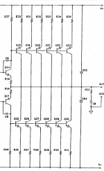
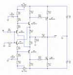
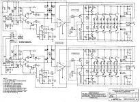
Very bad case.The output/power-stage from fig.2 (diamond-buffer-variations-juma_ha-f5-bjtin-gif) could look something like this from Threshold 300
While power output shoulder swithes off all load becomes coupled with driver stage.
Driver stage must off only after power output (instead it can't drive it) and this load switching produces very high crossover distortion, load variation to VAS stage (usually 100x times as of hFE of output devices) and also gain variation needed to be damped by feedback circuitry.
No. Bad OPS.
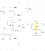
I've had diamond buffer circuits self-destruct because of thermal runaway. The Vbe of the input transistors was (surprise!) not identical to the Vbe of the output transistors.
And when the output transistors warm up, their Vbe falls (by that -2.2 millivolts per Kelvin number they keep hammering at school). The lower Vbe increases their collector current, which increases power dissipation, which increases junction temperature, which lowers Vbe even more, which increases collector current even more, ... you get the idea.
It's particularly annoying with TO-92 transistors whose thermal resistance ThetaJA is 175 Kelvin per watt. Blech.
A non-textbook approach that avoids thermal runaway is shown below. It works well in practice and is thermally stable. Quite stable in fact.
_
Attachments
Very bad case.
While power output shoulder swithes off all load becomes coupled with driver stage.
Driver stage must off only after power output (instead it can't drive it) and this load switching produces very high crossover distortion, load variation to VAS stage (usually 100x times as of hFE of output devices) and also gain variation needed to be damped by feedback circuitry.
No. Bad OPS.
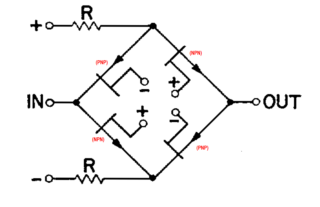
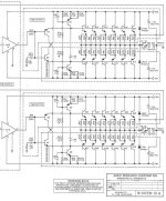
But the Threshold Stasis power-amps from Nelson Pass made a very good Job!
This schema is a cutout from the Threshold S300II Opto-Bias amp.
I have another Stasis schema with 70 (!) power transistors for each channel.


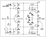
Ten years earlier, Audio Research D110B (1979) :The first Diamond Buffer comes from Walt Jung.
For a low power buffer, I then had the idea to connect the collectors of the input transistors to the emitters of the output collectors. When testing it, I met stability problems and did not persevere. Shame, the topology was valid !
I've had diamond buffer circuits self-destruct because of thermal runaway. The Vbe of the input transistors was (surprise!) not identical to the Vbe of the output transistors.
I'm surprised more isn't made of thermal stability in diamond buffers. You don't need a lot of Vbe mismatch to get into trouble -- at least in theory. It can be demonstrated using SPICE simulations as well.
For a current (very) small-signal project, I'm using the same method as you (extra resistance in the first stage emitters). I have yet to torture test it, but so far it's holding up.

Last edited:
The Diamond Circuit, by R. Baker, MIT Lincoln Laboratory. 1963 ISSCC Digest of Technical Papers, pp. 80-83.
Click on the image to see it full size and undistorted.
_
Click on the image to see it full size and undistorted.
_
Attachments
Last edited:
Member
Joined 2009
Paid Member
Ten years earlier, Audio Research D110B (1979) :
For a low power buffer, I then had the idea to connect the collectors of the input transistors to the emitters of the output collectors. When testing it, I met stability problems and did not persevere. Shame, the topology was valid !
I could not open your attachment - please take again
Sorry. I hope it is ok nowI could not open your attachment - please take again
Attachments
Ten years earlier, Audio Research D110B (1979) :
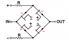
I'm not able to open your attachment, but I guess it is something like what I'm attaching.
Yes that is a true Diamond, quite brilliant.
Stein
Double posting.
Attachments
Last edited:
- Home
- Amplifiers
- Solid State
- Diamond Buffer variations