Hello to all.
I intend to assemble a NAP200 clone based on the ZeroZone PCB. But I got a doubt. Given that I have no problem getting BC239Cs but there is a technical reason why the Chinese in the NAP200 clones use the MPSA18s as TR1 and TR2 transistors instead of the BC239Cs or the choice is forced by the discontinued production of the BC239C. Furthermore, how should the MPSA18s be chosen? I saw that in the case of BC239C TR1 must be chosen with an HFE of 500 and TR2 of 430. In the case of MPSA18 what difference of HFE should I consider?
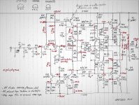
Ultimately I leave the MPSA18 or do I put the BC239C? For convenience I insert the scheme made by someone of good will on this site:
I intend to assemble a NAP200 clone based on the ZeroZone PCB. But I got a doubt. Given that I have no problem getting BC239Cs but there is a technical reason why the Chinese in the NAP200 clones use the MPSA18s as TR1 and TR2 transistors instead of the BC239Cs or the choice is forced by the discontinued production of the BC239C. Furthermore, how should the MPSA18s be chosen? I saw that in the case of BC239C TR1 must be chosen with an HFE of 500 and TR2 of 430. In the case of MPSA18 what difference of HFE should I consider?
Ultimately I leave the MPSA18 or do I put the BC239C? For convenience I insert the scheme made by someone of good will on this site:
Attachments
Last edited:
Of course. It appears from the datasheet. But what interests me is the differential configuration of the two transistors in question. I don't know what parameters to use and if you need to keep that configuration even though I guess logically yes. But I would have to go through a lot of trial and error selecting various pairs based on the difference in HFE and it's not exactly convenient.The MPSA18 are lower noise
@ian finch
can you help me?I've seen some of your advice on this
Last edited:
You may be over-thinking this. The OP circuit diagram by member algar-emi, is based on the bare PCB of a Chinese cloned NAP200 kit but the components supplied and shown on the overlay are not necessarily the same as those used in original NAP200 production models or other copied kits. They are suitable original part types that were still available to the kit supplier. BC239C may have been used by Naim in early models but it was not fitted in all products of that later, all black chassis period. BTW, Naim schematics were virtually all the same but the rail voltages were not so you need to be careful with using low voltage types like BC239.
I have seen a NAP200 and other models of the later period fitted with other BC series types too because the more important property to Naim was consistently high hFE in a narrow range to meet the 500/430 hFE constraint. They also returned a lot of product to suppliers for this reason but honestly, that's an expensive way to control DC offset and a sure-fire way to anger suppliers who won't have the facility or budget to sort those 2-cent, mass-produced semis.
Imagine that you just had a delivery of 10,000 new Transistors. How many would comply with that ridiculously tight specification? Maybe a few percent? No, that has to be wrong and the real picture is that Naim themselves tested each transistor and selected pairs for a differential that would result in a very low DC offset without adjustment. They even make a point of it in their forum posts, articles etc. The offset and reasonably low noise are the criteria and several small transistor types from various manufacturers were tried in order to get the best yield over the years.
Thanks for your very helpful post.
I have no difficulty switching to other alternative transistor pairs. I just wanted to understand if in the selection of the pairs I had to necessarily keep a ratio of 86 to 100 for the difference in HFE between the two transistors or I could go quiet without paying too much attention to the presence of significant differences in HFE between TR1 and TR2 because the DC control offset would be less critical due to the better characteristics of the transistors used.
I have no difficulty switching to other alternative transistor pairs. I just wanted to understand if in the selection of the pairs I had to necessarily keep a ratio of 86 to 100 for the difference in HFE between the two transistors or I could go quiet without paying too much attention to the presence of significant differences in HFE between TR1 and TR2 because the DC control offset would be less critical due to the better characteristics of the transistors used.
So even with the MPSA18 I can feel comfortable and use them without too many problems because they too have a minimum VCEO of 45VP.S. to #6
BC549C or BC550C from Taiwan semi or Onsemi are just fine as the input long-tail pair and they have better safety margins in that VCEO is 30V or 45V respectively, rather than the 25V of the BC239C.
Who wrote that ridiculous specification?I saw that in the case of BC239C TR1 must be chosen with an HFE of 500 and TR2 of 430.
Was it to control offset?
Wrong way, at such high Hfe and low idle current, base current through reference resistors, meaning R1+R2+R16 for Tr1 or R4 for Tr2 makes for minuscule drops since both values are quite low, around 27K.
To boot, both "should" drop the same , being about same current, about same resistive value, can NOT find a justification for the huge difference shown: 8mV vs 85mV
 UNLESS that comes from trying to compensate for a gross imbalance somewhere else in the circuit.
 I am guessing either a typo, or a mistaken measurement or maybe one transistor was freshly soldered and was still warmer than the other.
Also find ridiculous the 50ppm tolerance specs for resistors which frankly do NOT need to be that precise.
You say parts were rejected if not meeting those unreasonably tight specs?
Wow!!!!
Of course, *claiming* such high standards may help imbue buyers with awe and religious respect, good for sales
Or to "justify" high list price
Mind you, not berating the amp itself by any means.

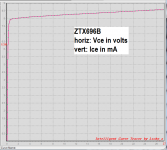
I've been using the Diodes Inc / Zetex ZTX696B in several Sony VFET front end card designs for the diyAudio Store. Maybe it might be a possible candidate for this application too (?)
Here is a link to the manufacturer's datasheet. Max voltage = 180V, current gain Beta = 500, max current = 500mA, max power dissipation = 1W thanks to Zetex's super duper "E-Line" plastic packaging technology.
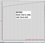
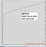
I put them on my curve tracer; results below. I only traced one curve for each transistor, the one that intersects 8 mA of collector current, because that was the operating condition which interested me at the time.
_
Here is a link to the manufacturer's datasheet. Max voltage = 180V, current gain Beta = 500, max current = 500mA, max power dissipation = 1W thanks to Zetex's super duper "E-Line" plastic packaging technology.
I put them on my curve tracer; results below. I only traced one curve for each transistor, the one that intersects 8 mA of collector current, because that was the operating condition which interested me at the time.
_
Attachments
Then. Let's go step by step. In the kit provided by the Chinese on duty are inserted silver mica capacitors that in such a circuit I would never put. Probably low values like the 10 pF and 39 pF capacitor are difficult to find in polystyrene but for most of the capacitors of critical value I found Styroflex from 63V to 1% at a few cents and that's okay. For the resistors I limited myself to those with a 1% Yageo and Vishay metal layer without too many problems. My goal was to equate as much as possible the values of the components in the two twin parts of the circuit which is basically a dual mono. What I would like to avoid is having to calculate from scratch all the sections of the circuit because otherwise I designed one from scratch and peace. That offset control system left me speechless too and that's why I asked those who have already had experience with this type of platform.Who wrote that ridiculous specification?
Was it to control offset?
Wrong way, at such high Hfe and low idle current, base current through reference resistors, meaning R1+R2+R16 for Tr1 or R4 for Tr2 makes for minuscule drops since both values are quite low, around 27K.
To boot, both "should" drop the same , being about same current, about same resistive value, can NOT find a justification for the huge difference shown: 8mV vs 85mV
I am guessing either a typo, or a mistaken measurement or maybe one transistor was freshly soldered and was still warmer than the other.
Also find ridiculous the 50ppm tolerance specs for resistors which frankly do NOT need to be that precise.
You say parts were rejected if not meeting those unreasonably tight specs?
Wow!!!!
Of course, *claiming* such high standards may help imbue buyers with awe and religious respect, good for sales
Or to "justify" high list price
Mind you, not berating the amp itself by any means.
Last edited:
The hFE ratio between TR1 and TR2 is only relevant to the DC offset that appears at the amplifier output. I find that a small amount of DC up to ~50mV is mostly a cosmetic matter that does not affect the speakers or the audio but when our imagination is fed with numbers of any size, we opt for precise, ideal settings when we have doubts or no clue what is relevant. 1V or more of DC could be disaster but perfect zeroing of the DC offset generally proves to be a waste of time and effort .
Re: "upside down" mounting of the transistors.
If you read more of the thread, you may realise that this became necessary with full-sized Naim amplifiers, in order to speed up the bias settling time (it could take 20-30 minutes in early models). Placing the differential transistor pair underneath the PCB brought them close to the the aluminium case which is also the heatsink (note the heat spreader bar under the power transistors) and as it happened, this greatly reduced settling time.
Accordingly, those transistors should be mounted on the underside anyway, regardless of how you orient the leads or insulate and twist them about to make the correct connections to them (which really is no problem when you can't see it . Take care with the length of the leads though, such that the transistors don't foul the bottom of the case when it flexes as you lift and place the amplifier on a shelf, for example. Note that the original product had special rubber PCB mounting posts which mechanically isolated the PCB and these also controlled the spacing between PCB and case. Check some of the pics of the real NAP200 on the internet, for reference.
Re: "upside down" mounting of the transistors.
If you read more of the thread, you may realise that this became necessary with full-sized Naim amplifiers, in order to speed up the bias settling time (it could take 20-30 minutes in early models). Placing the differential transistor pair underneath the PCB brought them close to the the aluminium case which is also the heatsink (note the heat spreader bar under the power transistors) and as it happened, this greatly reduced settling time.
Accordingly, those transistors should be mounted on the underside anyway, regardless of how you orient the leads or insulate and twist them about to make the correct connections to them (which really is no problem when you can't see it
. Take care with the length of the leads though, such that the transistors don't foul the bottom of the case when it flexes as you lift and place the amplifier on a shelf, for example. Note that the original product had special rubber PCB mounting posts which mechanically isolated the PCB and these also controlled the spacing between PCB and case. Check some of the pics of the real NAP200 on the internet, for reference.Part of that statement is verifiably true but it is more likely that the spread of hFE was simply not high enough to sort and get economical yields that met Naim's needs. If you read some of the interviews with Julian Vereker published on the the 'net, this was not the only deviation from normal engineering practice. So what though? Whatever nonsense and exorbitant costs Vereker invented by his delving into audio manufacture, customers agreed with the outcome and demanded the expensive little black box products on reputation.Who wrote that ridiculous specification?.......You say parts were rejected if not meeting those unreasonably tight specs?
Wow!!!!
Of course, *claiming* such high standards may help imbue buyers with awe and religious respect, good for sales
Or to "justify" high list price
Mind you, not berating the amp itself by any means.
Last edited:
Sorry folks, I got that wrong. The comments on upside-down mounting refer only to TR5, the VBE multiplier, not the diff. pair.Re: "upside down" mounting of the transistors.
If you read more of the thread, you may realise that this became necessary with full-sized Naim amplifiers, in order to speed up the bias settling time (it could take 20-30 minutes in early models). Placing the differential transistor pair underneath the PCB brought them close to the the aluminium case which is also the heatsink (note the heat spreader bar under the power transistors) and as it happened, this greatly reduced settling time.
Accordingly, those transistors should be mounted on the underside anyway, regardless of how you orient the leads or insulate and twist them about to make the correct connections to them (which really is no problem when you can't see it
which were actually shielded from air currents with a plastic cover.
Last edited:
I can also add a finding that some have made, it is that for an unknown reason (or that I have not read or heard yet), the PCB (s) are quieter on plastic pads or on metal pads but little or not tight (left a little free).
For Tr5, it depends if the box is "airtight" or not and large or not and it also depends on how and on what the power transistors are fixed.
The idea with Tr5 is to "capture" the heat from the power transistors as easily as possible.
For Tr5, it depends if the box is "airtight" or not and large or not and it also depends on how and on what the power transistors are fixed.
The idea with Tr5 is to "capture" the heat from the power transistors as easily as possible.
This I had guessed. In fact, I was about to tell you that the temperature compensation took place via TR5 installed under the PCB. The reverse I was referring to was due to the different pinout of the candidate transistors.Sorry folks, I got that wrong. The comments on upside-down mounting refer only to TR5, the VBE multiplier, not the diff. pair.
which were actually shielded from air currents with a plastic cover.
For the power transistors I use the Sanken 2SC2922. The cabinet is from Modushop the heavy non-dissipating steel that I modified by closing the slots in the bottom with an aluminum plate of about 3mm that I will use as a basis for the dissipation of the power transistors fixed on the other side by a robust wide copper bar 20mm high 10mm and 200mm long. In this way the heat diffusion below will be rapid and TR5 will be able to do its job.I can also add a finding that some have made, it is that for an unknown reason (or that I have not read or heard yet), the PCB (s) are quieter on plastic pads or on metal pads but little or not tight (left a little free).
For Tr5, it depends if the box is "airtight" or not and large or not and it also depends on how and on what the power transistors are fixed.
The idea with Tr5 is to "capture" the heat from the power transistors as easily as possible.
- Home
- Amplifiers
- Solid State
- MPSA18 VS BC239C