Perhaps I need to explain this another way. A star point is not a point. Its an area of 35um copper (quite a large area if you are handling 5A or so). Since its an area it doesn't fully isolate IR voltages on one trace from another trace. Its not a perfect point. With 5A and 35um copper this can mean mV levels of error unless great care is taken with physical symmetry. In a 100W amp each mV is 0.004% distortion so this can become the distortion floor.
The currents in the rails and decoupling caps are half-cycle - ie heavily distorted and large, so they are about the worst case.
However if they are summed you get a current that's basically linear (or at worst say 1% distorted) - routing this summed current to the star reduces any possibility of error at the star by 2 orders of magnitude or may be more - enough to become a non-issue.
This applies to the feedback pick-off point (after the emitter resistors merge, typically), and also to the feedback ground trace, which comes from a star point that should have a trace running to the merge-point for the decouplers. (At HF each decoupling cap carries the same heavy distorted half-cycle currents).
The power supply ground can go to the star point, or to the local decouplers' merge point, since it too has current that's linear with the signal (to a good approximation, and at LF especially).
And of course you have to worry about inductive coupling of rail / decoupler currents into the output inductor (its best mounted off board really).
Assuming your PSU and amp modules are separate (vast majority of DIY amplifiers), I'd recommend you try the following approach.
1. Position the output devices as required for heatsinking
2. Place the +, -, 0V speaker output and speaker return connectors close together, keeping in mind that the total loop area of the output bus (this is where the emitter degen resistors from the plus and minus half all join before going to the output coil) and their associated supply rails is minimized.
3. Keep the loop area between the 0V and the + and - supply rails small. This is best done on a double sided board by running the 0V directly underneath the + and - rail. Decoupling caps are mounted straight over the top of the two tracks
4. Bunch the HBR and gain setting resistor close together right near the amplifier front-end. Place the feedback resistor as close as possible to these other two resistors. The total loop area between the inverting input and these three resistors must be kept as small as possible in order to reduce noise and distortion (magnetically coupled)
5. Grounding order on the PCB wrt the main 0V connector (this is the 'T' method)
* main 0V to PSU
* speaker return
* decoupling cap return
* small signal 0V
* pick off to HBR - but note carefully that the track to the HBR resistor (which is located at the amplifier front end) must run right next to the signal 0V or on top of it - again this is to minimize the loop area.
On your main PSU PCB
1.A single thick 0V track connects the two main filter capacitors common. Absolutely nothing connects between the capacitors on this thick short track - there are large charging currents flowing through it and as a result, a noise voltage (100 Hz saw tooth) arises across it which you do not want getting into your amplifier through common impedance coupling. This track is the cross bar of the 'T'
2. Run a thick short track off at the centre of the cross bar (this is the 'I' part of the 'T')
3. First connection from this is to the chassis - there is one and only one connection to the chassis and this is it (either directly - preferred - or through a ground lifter)
4. Next is the 0V to the amplifier modules
Some people prefer to run their speaker return back to the central 0V on the PSU. If you do this, make sure the cable runs back alongside the speaker output cable, over the amplifier 0V track and is then bound tightly with the +, - and 0V. Again, all this in the interests of minimizing loop area. Keep the speaker return away from the front end/small signal circuitry. The speaker return in this method is placed just before the amplifier module 0V (ie closer to the 'T' cross bar)
The advantage of running the speaker return back to the module rather than the PSU board is that the loop areas are minimized and the loop formed by the speaker return and the module decoupling capacitors on the amplifier module is kept tight and loop inductance and resistance is minimized. There is no point in spending good money on low ESL/ESR caps only to throw it away through bad wiring plan practice.
Its important that the cables to the PSU are tightly bundled and cable tied. The output and speker return must also be tightly bound - I use 5mm cross section bonded speaker cable inside my amps for this reason - it minimizes any radiated fields.
When you lay the board out, start with the output bus and +- tracks (usually these will be going to the output device collectors)
Next place the decoupling capacitors
HBR, gain and feedback resistors
finally, rest of the amplifier tracks.
On a good layout, you should be able to get to -120 dBr on a small class AB amp, and 10 dB better than that on a large amp. This is typically -90 to -100 dBV.
Last edited:
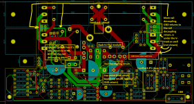
Here's my go at trying to make a tight layout for these issues - it shows a notional output stage with output devices and drivers and decoupling caps and big emitter resistors.
The feedback pick-off traces are going out to where the rest of the amp would be (only feedback resistors are shown). The pick offs come from the speaker terminal pads (the star points) opposite the main trace as my best effort at a 4-terminal connection to the load (which is another way to think of star points).
Loop area could be tighter by running traces on top on one another (for instance each rail could be under the ground trace), but that's harder to see clearly. The components at the left are Zobel network, I've omitted the inductor which might be off to the left or off the PCB entirely.

The supply traces keep close to each other and ground to reduce loop area broadcasting half-cycle magnetic fields - again running on top of each other might be even better.
I might have a go at doing a poor layout with all the layout faults I can think off as a comparison (though there are many examples out there of poor choice of feedback pick-off points if you look for it)
The feedback pick-off traces are going out to where the rest of the amp would be (only feedback resistors are shown). The pick offs come from the speaker terminal pads (the star points) opposite the main trace as my best effort at a 4-terminal connection to the load (which is another way to think of star points).
Loop area could be tighter by running traces on top on one another (for instance each rail could be under the ground trace), but that's harder to see clearly. The components at the left are Zobel network, I've omitted the inductor which might be off to the left or off the PCB entirely.
The supply traces keep close to each other and ground to reduce loop area broadcasting half-cycle magnetic fields - again running on top of each other might be even better.
I might have a go at doing a poor layout with all the layout faults I can think off as a comparison (though there are many examples out there of poor choice of feedback pick-off points if you look for it)
Last edited:
Here's my go at trying to make a tight layout for these issues - it shows a notional output stage with output devices and drivers and decoupling caps and big emitter resistors.
How is that sound?
Could you provide more information. Thanks.
Is your power supply (rectification/filter) and the amp on same board?
Where do you connect the ground for input signal? Use the same ground trace of feedback resistor?
Is the power supply regulated or not?
That's nice Mark - I think laying the power paths over the ground returns would be even better, but I understand you are showing the way forward here.
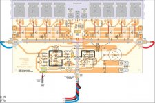
Here is a layout from a few years ago from a Silicon Chip design amp. Note how the ground and supply tracks are arranged. In this case, the designer ran the supply rails over the output bus to reduce the class B radiated loop areas. Because the transistors are not covered by the PCB, they missed an opportunity to further reduce the supply rail<>output bus loop area, but nevertheless quite good IMV.
Note this is a single sided PCB. With a double sided THP board (cheap as chips nowadays), the tracks would be on opposite sides of the board so no need for the cable gymnastics. Note the speaker output is also not optimized as we have discussed.
For a good example of a practical layout taking all these factors into account, see the Wolverine thread - the layout discussion is in the last c. 30 pages.
Attachments
Here is a layout from a few years ago from a Silicon Chip design amp. Note how the ground and supply tracks are arranged.
Is this a monoblock or stereo configuration?
There is only one ground connected to board. The signal ground is some what “bootstrapped” with big ground current. It is only good when used as monoblock.
Assuming your PSU and amp modules are separate (vast majority of DIY amplifiers), I'd recommend you try the following approach.
1. Position the output devices as required for heatsinking
2. Place the +, -, 0V speaker output and speaker return connectors close together, keeping in mind that the total loop area of the output bus (this is where the emitter degen resistors from the plus and minus half all join before going to the output coil) and their associated supply rails is minimized.
3. Keep the loop area between the 0V and the + and - supply rails small. This is best done on a double sided board by running the 0V directly underneath the + and - rail. Decoupling caps are mounted straight over the top of the two tracks
4. Bunch the HBR and gain setting resistor close together right near the amplifier front-end. Place the feedback resistor as close as possible to these other two resistors. The total loop area between the inverting input and these three resistors must be kept as small as possible in order to reduce noise and distortion (magnetically coupled)
5. Grounding order on the PCB wrt the main 0V connector (this is the 'T' method)
* main 0V to PSU
* speaker return
* decoupling cap return
* small signal 0V
* pick off to HBR - but note carefully that the track to the HBR resistor (which is located at the amplifier front end) must run right next to the signal 0V or on top of it - again this is to minimize the loop area.
On your main PSU PCB
1.A single thick 0V track connects the two main filter capacitors common. Absolutely nothing connects between the capacitors on this thick short track - there are large charging currents flowing through it and as a result, a noise voltage (100 Hz saw tooth) arises across it which you do not want getting into your amplifier through common impedance coupling. This track is the cross bar of the 'T'
2. Run a thick short track off at the centre of the cross bar (this is the 'I' part of the 'T')
3. First connection from this is to the chassis - there is one and only one connection to the chassis and this is it (either directly - preferred - or through a ground lifter)
4. Next is the 0V to the amplifier modules
Some people prefer to run their speaker return back to the central 0V on the PSU. If you do this, make sure the cable runs back alongside the speaker output cable, over the amplifier 0V track and is then bound tightly with the +, - and 0V. Again, all this in the interests of minimizing loop area. Keep the speaker return away from the front end/small signal circuitry. The speaker return in this method is placed just before the amplifier module 0V (ie closer to the 'T' cross bar)
The advantage of running the speaker return back to the module rather than the PSU board is that the loop areas are minimized and the loop formed by the speaker return and the module decoupling capacitors on the amplifier module is kept tight and loop inductance and resistance is minimized. There is no point in spending good money on low ESL/ESR caps only to throw it away through bad wiring plan practice.
Its important that the cables to the PSU are tightly bundled and cable tied. The output and speker return must also be tightly bound - I use 5mm cross section bonded speaker cable inside my amps for this reason - it minimizes any radiated fields.
When you lay the board out, start with the output bus and +- tracks (usually these will be going to the output device collectors)
Next place the decoupling capacitors
HBR, gain and feedback resistors
finally, rest of the amplifier tracks.
On a good layout, you should be able to get to -120 dBr on a small class AB amp, and 10 dB better than that on a large amp. This is typically -90 to -100 dBV.
Here's my go at trying to make a tight layout for these issues - it shows a notional output stage with output devices and drivers and decoupling caps and big emitter resistors.
The feedback pick-off traces are going out to where the rest of the amp would be (only feedback resistors are shown). The pick offs come from the speaker terminal pads (the star points) opposite the main trace as my best effort at a 4-terminal connection to the load (which is another way to think of star points).
Loop area could be tighter by running traces on top on one another (for instance each rail could be under the ground trace), but that's harder to see clearly. The components at the left are Zobel network, I've omitted the inductor which might be off to the left or off the PCB entirely.
The supply traces keep close to each other and ground to reduce loop area broadcasting half-cycle magnetic fields - again running on top of each other might be even better.
I might have a go at doing a poor layout with all the layout faults I can think off as a comparison (though there are many examples out there of poor choice of feedback pick-off points if you look for it)
Is this a monoblock or stereo configuration?
There is only one ground connected to board. The signal ground is some what “bootstrapped” with big ground current. It is only good when used as monoblock.
Thank you all for your input!! Bonsai, great explanation, very thorough, I really appreciate it. Over the next couple of days I will carefully take my time and collect all the tricks laid out in these posts, and apply it to my own layout. I am currently waiting on some copper wire for the output inductor, need to spec out the area the footprint will take out before I continue any further in layout.
Again... appreciate the knowledge transfer going on here, thank you to everyone.
Is this a monoblock or stereo configuration?
There is only one ground connected to board. The signal ground is some what “bootstrapped” with big ground current. It is only good when used as monoblock.
jxd, please read the ground loop presentation in the link below for a discussion on grounding. It’s quite permissible to have only one ground from the amplifier module to the PSU 0V in a stereo amplifier and get good results.
jxd, please read the ground loop presentation in the link below for a discussion on grounding. It’s quite permissible to have only one ground from the amplifier module to the PSU 0V in a stereo amplifier and get good results.
Bonsai,
I've given a go at a complete layout attempt. The order I proceeded was as follows:
1. incoming supply voltage terminals as close as possible in center
2. 2200uf local decoupling caps at these terminals create the "rail decoupling point" which goes directly to GND terminal (back to PSU module)
3. speaker output and return terminals are next to relay softstart circuitry
4. speaker return goes right to star point (right before the "rail decoupling point")
5. this star point is used for any other ground connections (other than zobel cap, which goes straight to speaker return), such as boostrap caps for CCS, the VAS transistor biasing (collector goes to GND), etc.
6. started on IPS
7. once IPS was somewhat in order - put feedback resistors and cap very close to inverting input
8. take feedback point from the ballast resistors (off of a T)
9. input stage ground is only connected to ground THROUGH HBR resistor, HBR resistor is located very close to IPS and track to GND runs to the star point
10. have a go at laying out the rest
where possible I tried running GND tracks under the supply tracks.
Here is a pic, let me know if anyone see's anything obviously wrong, or has any questions.
QUESTION: is it dangerous to have the feedback trace running under or near the big local decoupling caps?
Attachments
Hate to double post and bump this thread to the top, but didn't want to create a new thread for a simple question, apologies.
For signal ground at the preamp side, I currently have it set up in a configuration where it has a 100 ohm return path to the preamp local GND, which then stars back to the PSU ground.
Is this a bad idea? I'm realizing if I should not be returning signal ground AT ALL on the preamp side, and only let it happen through the amp board. Is this the correct approach? luckily all I would need to do is not populate the HBR 100 ohm resistor on the preamp board.
Thanks.
The problem is not lack of information. The problem is the information conflicting from different source. Which one you gonna follow. That is the question.
Here is a way to verify the correctness.
Try out the grounding scheme in simulation first. Put 1uH inductor and 0.1 Ohm in serial to all the power wire and ground wire, also add them to all the wires between the preamp and power amp.
Then use square wave to simulate. A good ground scheme should not cause extra overshooting at output.
You can also simulate power supply noise rejection using this method.
Apologies drinkingcube - missed this one. I am out for a few days - can you ping me mid next week and I’ll take a look (probably Thursday).
(Keep your HBR to =< 15 ohms. I’ve gone to 4.7 ohms now and great -120 dBr mains peaks perfectly achievable. High HBR values will only lead to problems.)
(Keep your HBR to =< 15 ohms. I’ve gone to 4.7 ohms now and great -120 dBr mains peaks perfectly achievable. High HBR values will only lead to problems.)
Last edited:
The problem is not lack of information. The problem is the information conflicting from different source. Which one you gonna follow. That is the question.
Here is a way to verify the correctness.
Try out the grounding scheme in simulation first. Put 1uH inductor and 0.1 Ohm in serial to all the power wire and ground wire, also add them to all the wires between the preamp and power amp.
Then use square wave to simulate. A good ground scheme should not cause extra overshooting at output.
You can also simulate power supply noise rejection using this method.
This is a good idea. I will try this when I have some free time.
Bonsai, no worries. Will send you a PM, but nothing is expected here, appreciate your help. When you say keeping HBR low, do you mean "in general", like on the amp board as well? Or is this specifically for the preamp section that you are referring to?Apologies drinkingcube - missed this one. I am out for a few days - can you ping me mid next week and I’ll take a look (probably Thursday).
(Keep your HBR to =< 15 ohms. I’ve gone to 4.7 ohms now and great -120 dBr mains peaks perfectly achievable. High HBR values will only lead to problems.)
- Home
- Amplifiers
- Solid State
- Signal Ground Question