I think... by exploiting self-heating and reducing the gain of the temperature probe circuit a bit, or by making a circuit that adds some bias when things get loud, it should be possible to get a resistor-free output stage that doesn't have any special non-switching circuit, but still doesn't make crossover spikes.
That's what the CircloMOS did, if I remember correctly.
I mean, crossover spikes appear when di/dt at turn-off goes over a threshold. But in music that never happens at the beginning of a transient. It happens at the first zero crossing after the transient. That leaves plenty of time to increase the bias. Also when it is loud, it spends little time in the crossover zone, which means the actual bias current is not being burned all the time, only at zero crossings, so increasing it briefly is almost free in terms of wasted power.
I completely agree: some "non-switching" topologies just keep the non- (or less-) active device conducting with an "alibi" quiescent current, but this doesn't help at all: at best it is neutral (think of a base series diode combining a small, fixed bias current with the real drive), and it can be counterproductive in more elaborate schemes using some kind of servo: each half of the PP tries to impose its set-quiescent current to the whole, resulting in a fight and a kind of inverse Xover distortion.In fact, the current that is kept on the device that does not turn off results in a sharper loss of transconductance for this device: even if it does not turn off, it is still out of the game, pretending to be off, so its transconductance becomes zero (black on the Ic fingerpainted curve below). But if it was allowed to use this extra current margin to turn off smoothly (blue) that would result in a smoother crossover. So, non-switching is a tradeoff: for the same static crossover distortion than a resistor-free BJT output, it needs more bias, but it makes no spikes.
Thus, the non-switching circuit needs to do something useful: keeping devices conducting isn't enough.
BJT's do not need revving up before they become active: they start almost instantly for AF timescales, and keeping them warmed-up just for the sake of it doesn't help (with maybe a small caveat in the light of your work: preventing large thermal excursions could help if the bias circuit isn't agile enough).
Turn-off is much more difficult, and deserves more attention, as you confirmed
Hi,
I think you pretty much need some small emitter resistance to use multiple devices in parallel. There are times you need more than one pair, and they tend to sound better as well. If you match the output transistors, that emitter resistance can be lower. Just an avenue for thought peufeu.
-Chris
I think you pretty much need some small emitter resistance to use multiple devices in parallel. There are times you need more than one pair, and they tend to sound better as well. If you match the output transistors, that emitter resistance can be lower. Just an avenue for thought peufeu.
-Chris

The old bench power supply I was using to power the test setup decided it was a good idea to output -50V instead of -15V, so all the expensive AD8421 instrumentation amplifiers went poof, along with most of the opamps. Amazingly, the TPA6120 survived. The micro also survived, since the positive power supply did not join in the screw up party.
Looks like I'm just gonna waste some time and money

But well, looks like it's time to order some parts, so I'm gonna get a pair of ThermalTraks, the smaller NJW0302/0281, and some spare FETs.
Order goes 6PM French time. I will try the schottky diode suggestion if someone recommends a particular diode before 6PM French time, feel free to make other suggestions if something comes to mind.
Firing up the hot air station...
Alright, all the fried devices are replaced, except the instrumentation amps... and the thing has a new +/-15V power supply based on LM317/337.
+1 for "alibi current"
In fact keeping them warmed-up would not help for thermal excursions, I think, because superposition...
Problem of using the non-switching circuit to do other things like adding feedback is... it's a nonlinear circuit, and the transconductance of all the semiconductors used in the feedback loop will depend on current going through them. Since it is part of their normal job to almost turn off, at this point they will be pretty slow, so compensation will be a headache, and it will make the whole thing slow, which means less feedback for the rest of the amp. I'm not convinced this is a profitable trade. I would rather have a fast output stage with a wide crossover.
To keep both features, we'd need a circuit that separates the common and differential mode drive for the output transistor bases:
Actual audio signal is common mode: it is the same on both transistor bases, or almost the same.
The correction voltage added by the non-switching circuit, which increases bias voltage a bit when needed, is the differential signal, since it is the voltage between the two bases.
So a non-switching circuit that acts only on this differential signal would preserve bandwidth. I think this can be done by putting the compensation caps on the input and using them to let high frequency pass through directly, skipping the non-switching circuit. I'll try to spice something.
Yes: without emitter resistors, not possible to parallel devices as the hotter one will get all the current. One could parallel device pairs by building say, two output stages and connecting their outputs together with low value resistors. That would preserve the desirable exponential crossover, but due to device mismatch, if they are driven by the same drivers, so they have the same base voltage, then one pair of devices will have more bias than the other. I'm not sure this is a problem. I'd have to compare two pairs biased equally, and two pairs biased unequally but with the same total bias current. A quick simulation should answer that.
I think it's possible to do it with resistor-free MOSFETs though, because the gate of a MOSFET has a very high impedance at DC it is much easier to add a pot to shift the drive voltage with a little bit of offset voltage for each FET, to null the mismatch. Not so with BJTs, you'd need one set of drivers per output pair to do this, because the pot has to be in a low current circuit.
I'm also going to order some low value SMD resistors...
Thus, the non-switching circuit needs to do something useful: keeping devices conducting isn't enough.
(...) keeping them warmed-up just for the sake of it doesn't help (with maybe a small caveat in the light of your work: preventing large thermal excursions could help if the bias circuit isn't agile enough).
+1 for "alibi current"
In fact keeping them warmed-up would not help for thermal excursions, I think, because superposition...
Problem of using the non-switching circuit to do other things like adding feedback is... it's a nonlinear circuit, and the transconductance of all the semiconductors used in the feedback loop will depend on current going through them. Since it is part of their normal job to almost turn off, at this point they will be pretty slow, so compensation will be a headache, and it will make the whole thing slow, which means less feedback for the rest of the amp. I'm not convinced this is a profitable trade. I would rather have a fast output stage with a wide crossover.
To keep both features, we'd need a circuit that separates the common and differential mode drive for the output transistor bases:
Actual audio signal is common mode: it is the same on both transistor bases, or almost the same.
The correction voltage added by the non-switching circuit, which increases bias voltage a bit when needed, is the differential signal, since it is the voltage between the two bases.
So a non-switching circuit that acts only on this differential signal would preserve bandwidth. I think this can be done by putting the compensation caps on the input and using them to let high frequency pass through directly, skipping the non-switching circuit. I'll try to spice something.
Hi,
I think you pretty much need some small emitter resistance to use multiple devices in parallel. There are times you need more than one pair, and they tend to sound better as well. If you match the output transistors, that emitter resistance can be lower. Just an avenue for thought peufeu. -Chris
Yes: without emitter resistors, not possible to parallel devices as the hotter one will get all the current. One could parallel device pairs by building say, two output stages and connecting their outputs together with low value resistors. That would preserve the desirable exponential crossover, but due to device mismatch, if they are driven by the same drivers, so they have the same base voltage, then one pair of devices will have more bias than the other. I'm not sure this is a problem. I'd have to compare two pairs biased equally, and two pairs biased unequally but with the same total bias current. A quick simulation should answer that.
I think it's possible to do it with resistor-free MOSFETs though, because the gate of a MOSFET has a very high impedance at DC it is much easier to add a pot to shift the drive voltage with a little bit of offset voltage for each FET, to null the mismatch. Not so with BJTs, you'd need one set of drivers per output pair to do this, because the pot has to be in a low current circuit.
I'm also going to order some low value SMD resistors...
Exactly: I name them orthogonal loops: the horizontal one is the regular signal path, and the vertical one controls the bias current.To keep both features, we'd need a circuit that separates the common and differential mode drive for the output transistor bases:
Actual audio signal is common mode: it is the same on both transistor bases, or almost the same.
The correction voltage added by the non-switching circuit, which increases bias voltage a bit when needed, is the differential signal, since it is the voltage between the two bases.
So a non-switching circuit that acts only on this differential signal would preserve bandwidth. I think this can be done by putting the compensation caps on the input and using them to let high frequency pass through directly, skipping the non-switching circuit. I'll try to spice something.
I used the concept in many amplifiers, both real and functional like the Circlophone, the Old-fashioned, the EZmos, and more experimental tentatives.
Ideally, the only coupling between the loops should be parametric: any direct spillover from one loop to the other causes distortion and problems.
That's the case with many auto-bias attempts, like Visch, and it generally has disastrous effects
Hi,
I think you pretty much need some small emitter resistance to use multiple devices in parallel. There are times you need more than one pair, and they tend to sound better as well. If you match the output transistors, that emitter resistance can be lower. Just an avenue for thought peufeu.
Without resistors, due to the exponential characteristic, one pair or several pairs have exactly the same crossover if the total bias current is constant. So that's the same as with MOSFETs with very low resistor values.
Of course two pairs at the same bias each as the original pair, for double total bias, would have lower distortion but the single pair can catch up by doubling its bias. Basically, parallelling reduces the distortion introduced by the ugly gm that is due to emitter resistors, but without emitter resistors, there is no problem. This leads to an interesting situation where paralleling reduces only the distortion introduced by the resistors that are needed for paralleling.
It is still nice to know that, without resistors, one pair at double bias will not be worse than two pairs at single bias (until it runs into hFe droop of course).
I've simulated two identical resistor-free BJT output stages joined to the output via 0.1R resistors. I added voltage sources in series with the bases to simulate a bit of Vbe mismatch between the devices.
1) If the PNP and NPN BJTs that have the lowest Vbe are paired together, this pair will have higher bias than the other. So it will have a wider crossover and turn off at higher current, but the other pair with lower bias will get the short end of the stick and turn off sooner. So the nice wide crossover without switching is lost. If all pairs share output current equally, which is the goal, the class-A zone will be determined by the pair with smallest bias.
Plus you get one set of turn-off spikes per pair for the same price
since they won't happen exactly at the same place. 2) If the transistors are sorted so the PNP with the high Vbe goes with the NPN with the low Vbe, so total Vbe per pair is constant, then each pair will have the same bias. That would be better. In this case, the simulator says it works perfectly if Vbe mismatch is reasonable between pairs, ie up to 40mV. The mismatch means some transistors will turn off earlier than others, but the di/dt will be divided by the number of pairs, and that is the cause of the crossover spikes, so that should more than compensate.
If the offset is much higher, like 0.2-0.3V it behaves just like Cordell's DoubleCross (a topology invented by many others too) and it produces a smoother crossover, but they will turn off at much lower current, so the non-switching feature is no longer available.
So yeah, it should be possible to parallel them, with a bit of matching, with an emphasis on equal bias current for each pair. If base resistors are replaced with ferrites, hFe matching should be unnecessary.
Attachments
Exactly: I name them orthogonal loops: the horizontal one is the regular signal path, and the vertical one controls the bias current.
I used the concept in many amplifiers, both real and functional like the Circlophone, the Old-fashioned, the EZmos, and more experimental tentatives.
Ideally, the only coupling between the loops should be parametric: any direct spillover from one loop to the other causes distortion and problems.
That's the case with many auto-bias attempts, like Visch, and it generally has disastrous effects
Easier said than done lol.
Let's continue this discussion about the non-switching bit in Ian's topic that he opened for this purpose...
I've given another look at the last measurement I made before it blew up.
If resistor-free output stages are paralleled, but the total bias is the same, does this improve turn-off spikes?
For: di/dt per transistor pair is halved.
Against: two pairs have 2x the capacitance and potentially 2x the stored charge, unless stored charge is exactly proportional to current, or something.
Neutral: at half the total bias each will have a narrower crossover per pair than one pair at full bias, which shouldn't matter since each handles one half of the current.
Does one compensate for the other? Unfortunately the answer is no: at the same frequency, the half bias output stage with half the output current is worse than the full bias stage with the full output current.
Therefore, paralleling loses some of its glitter... it increases current handling capability, but it worsens turn-off spikes.
(Assuming bias currents were accurate)
Meanwhile, the MOSFETs still don't have turn-off spikes.
Attachments
-
 scope-Bias=50.000 mA Iout=1.280 A F=24.000 kHz MJL1302-3281 v11 CFP Drivers Re=0 Rb=3R8 DrE=33R-.png263.3 KB · Views: 226
 -
 scope-Bias=100.000 mA Iout=2.560 A F=24.000 kHz MJL1302-3281 v11 CFP Drivers Re=0 Rb=3R8 DrE=33R.png256.1 KB · Views: 193
 -
 scope-Bias=50.000 mA Iout=640.000 mA F=12.000 kHz MJL1302-3281 v11 CFP Drivers Re=0 Rb=3R8 DrE=3.png261.8 KB · Views: 190
 -
 scope-Bias=100.000 mA Iout=1.280 A F=12.000 kHz MJL1302-3281 v11 CFP Drivers Re=0 Rb=3R8 DrE=33R.png257.5 KB · Views: 187
Last edited:
The replacement smoked chips have been shipped and should arrive tomorrow.
I will redo the above measurement to make sure the bias currents were exact. If that is confirmed, then the last two simple candidates (without fancy non-switching autobias) will be
- vertical MOSFETs
- BJTs without emitter resistors
Metrics to pick a winner:
- Gm smoothness, which is equivalent to high harmonics over the whole width of the crossover zone
- Turn-off spikes
- Current gain smoothness over the crossover zone
- Bandwidth
- Practicality
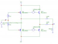
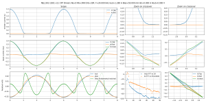
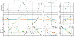
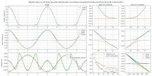
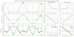
Diodes across the emitter resistors, as in Class-AC, per suggestion of OldDIY.
The idea is to make an output stage with highish emitter resistors and high bias, to get gm-doubling. Then, diodes+resistors are placed in parallel with the emitter resistors to also double gm with one transistor turn off, in the hope of having a constant gm across current.
This scheme requires that bias current * emitter resistor = diode turn on voltage, so with realistic (low) emitter resistor values this means a rather high bias.
Graph is nonlinear output impedance, which is the error voltage (ie, distortion) added by this output stage. That's 1/gm, so I put it upside down, and it looks just like gm...
Basically there is no way to make it flat, the parts don't stick together. And the transistors turn off early because of the high value resistors, which means turn-off spikes. I selected the least messy setting between bias and resistor values for presentation, but...
If it needs 300mA bias to work, then BJTs or MOSFETs without resistors (and thus without gm-doubling) have already won.
Attachments
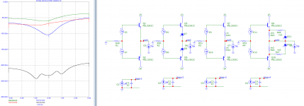
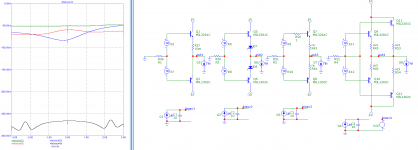
Now, class AC
I picked the best performing bias according to schematic values in the link. It needs a ridiculous 1.2A of bias current to work, and still does not deliver what it says: there is no gm-doubling, but when the class-C boosters turn on, they make a mess.
The other three output stages are simulated at 0.4A bias, so they waste 3x less power, and the resisto-free BJTs deliver much better performance. There really is no comparison. Besides, at this bias, it will run into hFe droop before it runs out of class A, so it can even get a class A sticker.
Attachments
Long time Qucs, Qucs-S and QucsStudio user.
I tried replicating your results in Qucs-S but Ngspice crashes.
I see .INCLUDE "C:/Program Files (x86)/Qucs-S/share/qucs-s/xspice_cmlib/include/ngspice_mathfunc.inc" in the netlist. Is this in the Qucs-S schematic? Qucs-S didn't place this in that location on my machine. Can you explain your setup?
Tom
This file should contain
* Ngspice functions
.func limexp(x) {x<80.0?exp(x):exp(80)*(x-80)}
.func step(x) {u(x)}
.func stp(x) {u(x)}
which should have installed with Qucs-S. Which version are you using? I am using 0.0.22.
Which version are you using? I am using 0.0.22.
I'm using Qucs-S 0.0.22. The inc file is the same but it's in a different location than yours but that doesn't seem to be the problem.
The version of ngspice I am using may be different. I used the one posted on the Qucs-S webpage which is ver 26?. They claim other versions won't work.
I got everything BUT the C300 VDMOS schematics to work but I had to edit all the .MODEL statements to remove "mfg=XXXX". I read the Bob Cordell models work in LTSpice. I don't know how you got the Bob Cordell models to work in ngspice.
I am using version 32.
ngspice - Browse /ng-spice-rework/old-releases/32 at SourceForge.net
I put it in D:\ngspice-32_64ngspice compiled from ngspice revision 32
Written originally by Berkeley University
Currently maintained by the NGSpice Project
Copyright (C) 1985-1996, The Regents of the University of California
Copyright (C) 1999-2011, The NGSpice Project
Guys ngspice isn't the topic, you can do that via PM.
Reichelt sells a ton of Chinese clones of mythical Japanese transistors at pretty cheap prices.
I'm going to order a few.
Anybody got a pair of the good fast SanKen's to lend me?
Reichelt sells a ton of Chinese clones of mythical Japanese transistors at pretty cheap prices.
I'm going to order a few.
Anybody got a pair of the good fast SanKen's to lend me?
I am using version 32.
I put it in D:\ngspice-32_64
Thanks it worked and ngspice is much faster
- Home
- Amplifiers
- Solid State
- Power amp OUTPUT STAGE measurements shootout