Oak Leaf - YABI (Yet Another Blameless Implementation)
I'm happy to pick up on my hobby/passion of tinkering with electronics projects after a gap of over 30 years.
Decided on making a Power Amplifier for home use with the following broad design considerations:
1). 150W RMS Power into 8 Ohms.
2). 4 Ohms driving capability (I believe that would be 260W into 4 Ohms).
3). THD within 0.05% at 250W RMS at 4 Ohms and 20KHz.
4). Least number of components to achieve the above.
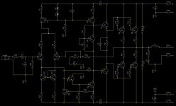
It seemed to me that the blameless design would fit the bill. In any case, this design is one of the most detailed and documented out there. Hence went along with it.
I have tried to pick the simplest but effective design elements for each of the stages (Input / VAS / Output), to come up the the prototype that I am now posting.
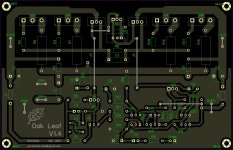
I also went ahead and made the PCB layout just for the sake of completion, and also to help me learn the software that I used for the purpose.
I would love to hear what I have done right, and of course what can be improved both in terms of the schematic and the PCB layout.
I'm happy to pick up on my hobby/passion of tinkering with electronics projects after a gap of over 30 years.
Decided on making a Power Amplifier for home use with the following broad design considerations:
1). 150W RMS Power into 8 Ohms.
2). 4 Ohms driving capability (I believe that would be 260W into 4 Ohms).
3). THD within 0.05% at 250W RMS at 4 Ohms and 20KHz.
4). Least number of components to achieve the above.
It seemed to me that the blameless design would fit the bill. In any case, this design is one of the most detailed and documented out there. Hence went along with it.
I have tried to pick the simplest but effective design elements for each of the stages (Input / VAS / Output), to come up the the prototype that I am now posting.
I also went ahead and made the PCB layout just for the sake of completion, and also to help me learn the software that I used for the purpose.
I would love to hear what I have done right, and of course what can be improved both in terms of the schematic and the PCB layout.
Attachments
Last edited:
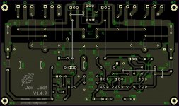
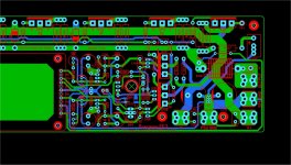
Your feedback pick-off point isn't in the right place, so you'll see unwanted IR voltages from resistive nature of the output trace imposed on your signal.
I'd take pick-off from below the (square) pad for the inductor to R18.
You also have the ground pick-off non-optimal - you don't want large currents in the ground trace/plane between the speaker ground and input section - run a star-ground from the speaker ground terminal to the input section so its sensing exactly the speaker signal.
The C9 decoupling cap will be seeing current pulses that are half-cycles and this will be imposed on the groundplane between the speaker terminal and the input section.
Its easy to assume a PCB trace has zero resistance, but for an amplifier driving a 4 ohm load and hoping for 0.001% distortion you are asking the traces to have less than 4/100000 ohms (40 µohms) if you allow half-cycle currents in them.
1oz copper pcb hase about 500µohms/square, so a trace thats 10 times longer than wide is about 5mohms, or about 0.1% of the speaker impedance.
Preventing non-linear currents in the traces/plane between speaker terminals and input section means these resistances are not going to affect linearity.
Thank you for the inputs.
Yes, the audio pick up point was shifted to the left to separate out the high current sections from the low current sections (hence the two Grounds). I thought it a 5mm track would probably handle not make it too bad, but I can pick the speaker output off the 5mm track from its mid point and shift eh zobel network probably on an external board (which I was avoiding), which would move the layout closer to the star arramgement that you are suggesting.
Yes, the audio pick up point was shifted to the left to separate out the high current sections from the low current sections (hence the two Grounds). I thought it a 5mm track would probably handle not make it too bad, but I can pick the speaker output off the 5mm track from its mid point and shift eh zobel network probably on an external board (which I was avoiding), which would move the layout closer to the star arramgement that you are suggesting.
Totally agree! That's what my reply to Mark above is based on. I kept the output takeoff to the left to segregate the high current parts with the low current parts. I did assume that a 5mm track would handle it enough to keep the THD within my target range 0.05%
The output takeoff can be moved to the middle of the 5mm track to keep it pure. However that might necessitate moving the zobel network off this board to another one.
The output takeoff can be moved to the middle of the 5mm track to keep it pure. However that might necessitate moving the zobel network off this board to another one.
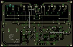
Made a layout change to the tracks for the output stage. Brought most of them in front of the transistors. Previously they were routed from behind the transistors.
This has two advantages:
a) The output transistors are now nearer the PCB edge. Better for heatsink mounting.
b) The board height reduced making it a bit more compact.
This has two advantages:
a) The output transistors are now nearer the PCB edge. Better for heatsink mounting.
b) The board height reduced making it a bit more compact.
Attachments
Made a layout change to the tracks for the output stage. Brought most of them in front of the transistors. Previously they were routed from behind the transistors.
This has two advantages:
a) The output transistors are now nearer the PCB edge. Better for heatsink mounting.
b) The board height reduced making it a bit more compact.
L1 and R18 must terminate on the same trace , in the middle.
OS
One big ground plane is not ideal in audio amp like this. Use star grounding point and route dirty grounds on their own tracks to the star. You can still ground plane the input stage. After all critical grounds have been routed separately.
I can break the ground plane into multiple "zones". I assumed that physical proximity of the devices to the corresponding ground terminals (there are two of them) would suffice. The current will follow the shortest path (path of least resistance).
consider L1 as a EMP "nuke" sitting close to your sensitive input stage.
I don't do symmetric power and output boards no more. 90% percent
of DIYA layouts do not enhance circuit performance.
My L1 is in the "dirty" power section. (below)
Ground planes have nearly no place on audio PCB's ... antenna's !!
PS - 3 distinct grounds. Input and NFB reference to the speaker ground.
Power supplies and internal IPS reference to G1 (main PS ground) ,
Chassis ground is the sum of the former .... G2 is derived from G1
at the via's where the half wave return pulses from the main caps cancel out.
Ground is the amps "master reference" , more important than even the power supply. The amps design can be twisted to consume a very dirty PS.
OS
Attachments
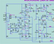
Consider the ease to "go all the way" (below).
Cascodes mitigate local miller effects , allow low voltage mirrors and
LTP devices.
Clip diode D3 will keep it from burning up.
Any of the extra's will enhance "the blameless experience" considerably.
OS
I still need to wrap my head around cascodes, so I tend to use higher voltage transistors instead
I did implement current limiting in the VAS section.
consider L1 as a EMP "nuke" sitting close to your sensitive input stage.
I don't do symmetric power and output boards no more. 90% percent
of DIYA layouts do not enhance circuit performance.
My L1 is in the "dirty" power section. (below)
Ground planes have nearly no place on audio PCB's ... antenna's !!
PS - 3 distinct grounds. Input and NFB reference to the speaker ground.
Power supplies and internal IPS reference to G1 (main PS ground) ,
Chassis ground is the sum of the former .... G2 is derived from G1
at the via's where the half wave return pulses from the main caps cancel out.
Ground is the amps "master reference" , more important than even the power supply. The amps design can be twisted to consume a very dirty PS.
OS
Aha! now you tell me about the symmetric eh?
Yeah I thought as much on the overall effect on distortion that a lack of symmetry would impact. Hence the asymmetric speaker output point. I however don't have measurement instruments which would help confirm this, so I have to go with the design descriptions given in books and the feedback that I receive from folks like yourself.
I thought ground planes should help, so that's actually a surprise there.
Btw, the pcb screenshot you shared, is this your blameless implementation?
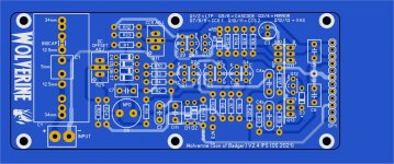
Yes , going to be the store amp.
You can swap out any design there is to it. It is just a EF3 power stage.
OS
Oh Nice! Looks like a double layer board.
Btw is Wolverine your design? Pardon the ignorant question, I'm new around here, but I have indeed heard about Honey Badger and Wolverine. They seem to be quite the rage in audio circles.
As a matter of fact, in my previous versions, I had put in pots for:
a) DC Offset adjustment
b) Gain adjustment
c) Bias adjustment
Someone told me that pots go bad over time and thus should be avoided. Hence I dropped (a) and (b) above, keeping only (c). What is your take on this?
- Home
- Amplifiers
- Solid State
- Oak Leaf - YABI (Yet Another Blameless Design)