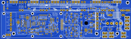
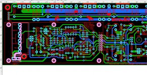
Looks Great OS, You need a outline on layer 0 that surrounds the pcb. This is what the pcb companies use to cut the board to not just sizing the properties of your pcb workspace within sprint layout.
Ahh , layer O.
Tweaked the cap , layer O.
.8mm for to-92 , 1mm for 1/4w , most everything else ... JW's 1.7mm.
I don't see how anything can be undersized.

OS
Attachments
Still no outline that I can see have a look at post 407. Open the sprint layout fileAhh , layer O.
Tweaked the cap , layer O.
.8mm for to-92 , 1mm for 1/4w , most everything else ... JW's 1.7mm.
I don't see how anything can be undersized.
OS
View attachment 942153
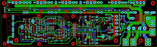
I guess it depends on what colour you you have layer 0 set to.Its that black line around the board.
Or the green one in this export.
OS
I have mine set to white.
If you open my sprint file and change the color of the outline (layer 0) to white you will see my outlines. They also have a radius in the corner. Should be easy to see.
You can always load your fab files up on jlcpcb, when you do the quote, it does a file check, displays the gerber and auto calc your pcb size. Need to name the files appropriately according to their naming conventions, put in a zip file.
If you want I can review the fab data, send me the nda and i’ll sign it if you want this free service I do it for every design I do, modern day convieniences = slick
If you want I can review the fab data, send me the nda and i’ll sign it if you want this free service
I do it for every design I do, modern day convieniences = slick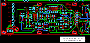
You guys should really consider moving up to some better software! Sprint just doesn't have the capabilities to do the job efficiently. Way too easy to make a mistake. Any decent software will verify connections match the layout. Most do decent 3D renderings to ensure things actually fit. Let Sprint die with the TO-92 transistors!
Main board DIP1 offset 1mm (up).Please take a look at this OS. I tried lining up the standard IPS over the last sprint file you posted V1.5 in post 423 and it doesn't line up.
Your other shift to the left is because you lined up the wrong row on dip one.
Standard IPS.lay is right on.
JW , Can't afford software. Barely afford the hardware.
OS
I agree, sprint layout is not bad for a quick hack. But Kicad is the way to go. I learnt it in a little over a week.Main board DIP1 offset 1mm (up).
Your other shift to the left is because you lined up the wrong row on dip one.
Standard IPS.lay is right on.
JW , Can't afford software. Barely afford the hardware.
OS
This was my first design.
Prototype... schematic... 3D model... final design...


You guys should really consider moving up to some better software! Sprint just doesn't have the capabilities to do the job efficiently. Way too easy to make a mistake. Any decent software will verify connections match the layout. Most do decent 3D renderings to ensure things actually fit. Let Sprint die with the TO-92 transistors!
Now ...with the native "mind check" of manual sprint under my belt , how good
would I be with advanced software ?
Also , this experience is quite valuable. Most here (usa south) know not even what a mm is.
I was looking at big caps , they have the dimensions in inches.
I don't do inches !!!
Yeah , It's getting "lopsided" - SMD now beats through-hole 7800/2300 for the
Mouser discrete count.
Poor , Poor DIYA . Look at the forum. Tubes.. wires , no SMD kits ??
I am personally quite open to the "hybrid" (below). Spooky and Hellraiser
especially would be good to start. Would not want to be a "luddite".
Even with SMD , perhaps a little "Luddity" might be good.
I could actually fix my present Xeon V3 MB , with its D-pak's and sot-23's.
My sons new MB ??? I can barely even see the components. Disposable ??
OS
Attachments
Last edited:
"Standard" fits wolverine - KICAD
(Below) perfect fit now. Row 2 !! of DIP1 is where it goes. Macro'ed "standard"
holes line up perfect.
Kicad - says won't work on my W7. BS , I have corp. extended support
patches on my 7. Digital signing,AES is just like 8/10.
I go on my son's W10 PC , 7 is all buried in it. M$ just took 7 and "adafied"
it .... no innovation - just a sellout. (below 2}
Kicad is like Eagle + , big modern library ... lots of chips.
Guess I'll learn it.
Perfect Wolverine attached , as well.
OS
Attachments
Big difference between a carpenter C-hair and a machinists C-hair!
Then there is the PCB C-hair.
OS
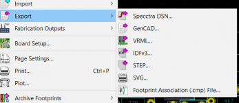
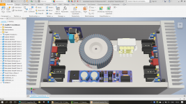
I've been curious about Kicad but haven't had time to play with it. Are you able to export a .dxf from the 3D rendering in it? This is a handy option to use with Fusion for chassis design!
I export to STEP and import into CAD, Im using Autodesk inventor, but Fushion 360 is about the same.
Ive attached a STEP exported from KiCad so you can import into Fusion to see for yourself.
Regards
Attachments
- Home
- Amplifiers
- Solid State
- DIYA store "Wolverine" (Son of Badger) .... suggestions ??