Howdy;
I just joined the DIY Audio fora. I posted on the introductions forum but the short version is...
I earned a BS in electrical engineering in the 1980s and have never really used it. I am currently unemployed so am using some of my time to try relearning the vast amount of forgotten material, which leads me to this post.
I intend to get into tubes but lack of money has me playing with the stuff that I already have in the junk drawer. I have prototyped a class AB power amp of about 10-15W and have it running but until I get the money for the finishing touches I have a 2N3055 laying begging to be put to use.
My plan is to make a small SE class A power amp. I have several small signal transistors of both the NPN and PNP persuasion as well as one N channel JFET. The first version will not use any fancy current sources etc because I want to keep it simple and because I have only one power transistor available. Later on who knows.
Currently I am thinking of using either an NPN or the jFET for an input stage (VD biased CE for the NPN or source bias CS for the jFET) and an emitter follower output stage. I am considering a PNP CE for the driver or using the PNP to make a complimentary darlington with the 2N3055.
Any thoughts on the basic plan?
Also I have been unable to find charateristic curves for the 2N3055. Is there a rule of thumb for setting the bias current in this kind of amp?
Welcome to the forum.
SE class-A output stage, set your bias to about 2x your peak target output current. So, if you want 5-watts into 8-ohms, set it to around 1-amp. Better find a good heatsink though.
For the input stage, you can go with a lot less bias. Common values are 1mA to 5mA. In my oppinion, setting the bias current in the input stage has more to do with getting the output impedance and DC level right for driving your output stage than other stuf.
For a datasheet, check out MJE3055, I think they should be similar devices.
I also suggest looking at the Pass Zen amp. It's a SE class-A amp you might consider adapting.
--
Danny
thanks
Thanks for the input. I have data sheets for the 3055. There are a lot of curves related to max ratings and switching applications but no characteristic curves (Vc v.s. Ic) analogous to the plate curves on a tube. Maybe the devices vary so much that you have to run the traces for each individual device.
In any case we are thinking along the same lines. I was thinking 1 to 1.5A depending on where I end up with PS voltage (probably 15V). For heatsinks the transistor is already mounted on a small four fin heatsink (it was used on a 4 amp 12V power supply) and I have a larger 8 fin heat sink which is about three times the size of the original. I may be able to bolt the existing heat sink to the larger one but I may need to just move it to the new heatsink.
I will check out the Pass. I think that is a single stage mosfet design if I remember right.
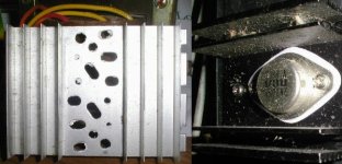
I am trying to post an attachment with this. It is a picture of the heatsinks.
Thanks for the input. I have data sheets for the 3055. There are a lot of curves related to max ratings and switching applications but no characteristic curves (Vc v.s. Ic) analogous to the plate curves on a tube. Maybe the devices vary so much that you have to run the traces for each individual device.
In any case we are thinking along the same lines. I was thinking 1 to 1.5A depending on where I end up with PS voltage (probably 15V). For heatsinks the transistor is already mounted on a small four fin heatsink (it was used on a 4 amp 12V power supply) and I have a larger 8 fin heat sink which is about three times the size of the original. I may be able to bolt the existing heat sink to the larger one but I may need to just move it to the new heatsink.
I will check out the Pass. I think that is a single stage mosfet design if I remember right.
I am trying to post an attachment with this. It is a picture of the heatsinks.
Attachments
Ah, well, I'm not too familiar with tubes although sometimes I wish I was. I doubt I'll get obsessed with the "tube sound" but they just seem fun to play with.
Anyway, a Vc vs Ic curve would depend on the collector loading. What you're really asking is probably: Ic vs Ib curve since a BJT is a current focused device. And that curve is very dependant on Beta which is completely not a controlable factor. You're better off being aware of what the curves kind of look like and then making sure you stay in the fwd-active region. Mostly you want to try and work around beta as the gain factor in your circuit. gm = Ic/Vt and Av = -gmRc for a CE amp.
1-amp, 15-volts = 15watts dissipated. That heatsink may do it, bigger is better... I found that my first time doing a zen, I way underestimated my power consumption and heatsinking needs. Bang-for-buck your best bet is to go to a computer parts store and try and find a cheap, obsolete Athlon heatsink to start with.
You're right, Pass Zen is a single stage mosfet amp, I was suggesting you make a BJT version, it might be interesting. I'd like to see one. But the Zen uses an active current source so I guess that's not quite what you're thinking yet but it's a good start.
--
Danny

Welcome to DIY. You might find inspiration and material in the threads devoted to the Class-A amp of John Linsely Hood. There are a couple I know of and the main one had over 900 posts at the last count. His design is 10-20 watts and the later versions specified 2N3055's. If you have not browsed in this DIY forum before his work is usually refered to by his initials (JLH) and if you put "JLH" and "class A" in "search" you should get several threads. The other place to go is a site maintained by one of the DIY Members and it is devoted to the amp just refered to. Try www.tcaas.btintenet.co.uk. "Class-A amplifier" in Google will give it as the first option (I.E. Geoff's site) and later sites on page one will give you Elliot Sound Products that feature the JLH design and other class-A units. The latter site is in sunny Australia. Jonathan Bright (Australia)
the jlh 1969 is a simple circuit to build and has the advantage of higher efficiency. I have tried quite a few versions of it with great results. it can also be done with your existing transistors.
you can also put together one of those Zen amps: they are quite simple. I especially liked the latest Zen with feedback (I have a similar design like it but has only one half. It is in one of those pre-amp threads). the zens are mostly (all?) based on mosfets but you can also use the 3055 as well.
as to datasheet, you can try onsemi or fairchild, to name a few.
millwood said:you can also put together one of those Zen amps .................. the zens are mostly (all?) based on mosfets but you can also use the 3055 as well.
Really?

Is the 2N3055 a drop-in replacement for the IRFP140? If not, what circuit modifications do you suggest would be necessary to make it work, whilst maintaining similar performance (distortion, output power etc).
Here is where my head is
Jonathan, thanks for the tip on the JLH. I will check it out.
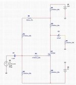
I thought that it might be useful to look at a couple of circuits. The top circuit in the attached jpeg is a priliminary sketch of my thoughts for the class A amp. The bottom circuit is the current state of a class AB prototype on which I am working. I am including this second circuit so that you can get an idea of from whence I am coming. I would welcome comments on both circuits (and my interpretation of them). Please be gentle... I am trying to learn here.
The Class AB Amp:
this is a modification of a design from an old text book. The values in () are the actual values as I built it. The indicated voltages are actual measured values in the prototype. Just noticed that the schematic shows R1 = 50k pot. This has been changed to 100k. Note that the original design used two diodes in place of the 390 ohm bias resistor. I was having trouble getting the right bias with the diodes and so I switched to a resistor (I was using rectifier diodes which may have been the problem). When everything else is sorted out I will probably try using signal diodes (or a single diode with a trim pot).
As it now sits the prototype idles very cool and when played quite loudly the heatsink gets warm but not at all uncomfortable to touch continuously. It sounds fairly good at moderate to high volume levels. If I drive it with a signal low enough that I have to put my ear right up next to the speaker to even hear it I hear some static like distortion (cross-over distortion?).
Given that the amp idles as cool as it does and the distortion at very low signal levels I suspect that I might be more like class B at this point. This may not be a big deal since it will be used as a utility amp for an electronic keyboard but the goal is Class AB.
I am also concerned with the low voltage at the base of Q1 since this will limit the input voltage headroom. I am able to drive it to a nice level with a cassette deck but I would feel more comfortable with a little more voltage swing. I did not increase R3 very much from the original design and I probably should double it to get a bit more headroom (and better Zin) and then readjust R1.
I also note that I could have (should have?) used small signal devices for Q2 and Q3 but the TIPs were handy and I thought that the extra current and power capability would give me some extra leeway. I may change them out and use the TIPs to make another identical channel.
One thing that I had trouble with initially was understanding the purpose and operation of C2. The text book claimed that it was used to decouple the PS by bypassing R6. Now it doesn't look to me like this is the case at all. From other reading that I have done I think that it is used to bootstrap R4. Am I off base here?
The initial circuit did not have the Zobel. I threw that in when I thought that I might be getting ultrasonic oscillation (I still am not sure and I don't have a scope to check it out).
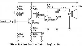
The Class A Circuit (V+ = 15V):
Now be kind... I am doing this in order to learn remember.
Since this is a learning project I thought that I would try something a little different and use an EF output stage and build the first version with no interstage feedback. The circuit shown is my first concept of what it would look like.
Icq3 will be set to approximately 1A. From 2N3055 data sheet hFE@Ic=1A@25deg.C is 90 ==> Ibq3=11mA so Icq2 should be about 100mA to prevent excess loading by Ibq3.
The first thing I notice is that Vcq2 will be (V+/2)+ 0.6 = 8.1V in this case. Now the maximum input to Q2 will be limited by the Quiescent voltage across Re2 which is limited to substantially less that V+/2 due to the requirement that the C-E junction remain reverse biased. This should be OK as long as we give the Q2 stage sufficient gain to bring this up to near the supply voltage(???). Will I be able to get a gain of about 5 in the Q2 stage while still being able to deliver sufficient drive current for Q3? Would I choose Re2 such that Veq2=(V+ - Vbq3)/2 or should I use higher voltage gain in Q2 (and lower Vdrop in Re2) so that I can maximize Vcq2 swing? As you can see I am a little bit confused on how to optimize this.
My initial impulse was to collapse the Q2/Q3 stage into what I would call a complementary darlington pair (like a darlington but using PNP-NPN pair) but unless I am missing something this appears to be impossible with an EF output stage because of the severe limitation on the input voltage (Q2 emitter is at V+). A true darlington using 2 NPN devices possibly?
The pot connection of C4 is for prototyping purposes so that the gain of stage one can be adjusted.
So am I totally out in left field here? Barking up the wrong pole?
Jonathan, thanks for the tip on the JLH. I will check it out.
I thought that it might be useful to look at a couple of circuits. The top circuit in the attached jpeg is a priliminary sketch of my thoughts for the class A amp. The bottom circuit is the current state of a class AB prototype on which I am working. I am including this second circuit so that you can get an idea of from whence I am coming. I would welcome comments on both circuits (and my interpretation of them). Please be gentle... I am trying to learn here.
The Class AB Amp:
this is a modification of a design from an old text book. The values in () are the actual values as I built it. The indicated voltages are actual measured values in the prototype. Just noticed that the schematic shows R1 = 50k pot. This has been changed to 100k. Note that the original design used two diodes in place of the 390 ohm bias resistor. I was having trouble getting the right bias with the diodes and so I switched to a resistor (I was using rectifier diodes which may have been the problem). When everything else is sorted out I will probably try using signal diodes (or a single diode with a trim pot).
As it now sits the prototype idles very cool and when played quite loudly the heatsink gets warm but not at all uncomfortable to touch continuously. It sounds fairly good at moderate to high volume levels. If I drive it with a signal low enough that I have to put my ear right up next to the speaker to even hear it I hear some static like distortion (cross-over distortion?).
Given that the amp idles as cool as it does and the distortion at very low signal levels I suspect that I might be more like class B at this point. This may not be a big deal since it will be used as a utility amp for an electronic keyboard but the goal is Class AB.
I am also concerned with the low voltage at the base of Q1 since this will limit the input voltage headroom. I am able to drive it to a nice level with a cassette deck but I would feel more comfortable with a little more voltage swing. I did not increase R3 very much from the original design and I probably should double it to get a bit more headroom (and better Zin) and then readjust R1.
I also note that I could have (should have?) used small signal devices for Q2 and Q3 but the TIPs were handy and I thought that the extra current and power capability would give me some extra leeway. I may change them out and use the TIPs to make another identical channel.
One thing that I had trouble with initially was understanding the purpose and operation of C2. The text book claimed that it was used to decouple the PS by bypassing R6. Now it doesn't look to me like this is the case at all. From other reading that I have done I think that it is used to bootstrap R4. Am I off base here?
The initial circuit did not have the Zobel. I threw that in when I thought that I might be getting ultrasonic oscillation (I still am not sure and I don't have a scope to check it out).
The Class A Circuit (V+ = 15V):
Now be kind... I am doing this in order to learn remember.
Since this is a learning project I thought that I would try something a little different and use an EF output stage and build the first version with no interstage feedback. The circuit shown is my first concept of what it would look like.
Icq3 will be set to approximately 1A. From 2N3055 data sheet hFE@Ic=1A@25deg.C is 90 ==> Ibq3=11mA so Icq2 should be about 100mA to prevent excess loading by Ibq3.
The first thing I notice is that Vcq2 will be (V+/2)+ 0.6 = 8.1V in this case. Now the maximum input to Q2 will be limited by the Quiescent voltage across Re2 which is limited to substantially less that V+/2 due to the requirement that the C-E junction remain reverse biased. This should be OK as long as we give the Q2 stage sufficient gain to bring this up to near the supply voltage(???). Will I be able to get a gain of about 5 in the Q2 stage while still being able to deliver sufficient drive current for Q3? Would I choose Re2 such that Veq2=(V+ - Vbq3)/2 or should I use higher voltage gain in Q2 (and lower Vdrop in Re2) so that I can maximize Vcq2 swing? As you can see I am a little bit confused on how to optimize this.
My initial impulse was to collapse the Q2/Q3 stage into what I would call a complementary darlington pair (like a darlington but using PNP-NPN pair) but unless I am missing something this appears to be impossible with an EF output stage because of the severe limitation on the input voltage (Q2 emitter is at V+). A true darlington using 2 NPN devices possibly?
The pot connection of C4 is for prototyping purposes so that the gain of stage one can be adjusted.
So am I totally out in left field here? Barking up the wrong pole?
Attachments
Re: Here is where my head is
That would be called a "CFP" or complementary feedback pair. It's a pretty common type of output stage. While most used strictly for output stages try to create unity gain, there are versions that actually have gain. A CFP wouldn't be a bad idea to try, it looks similar to what you're doing now anyway. So a search on CFP or sziklai pair for more info.
--
Danny
mashaffer said:
My initial impulse was to collapse the Q2/Q3 stage into what I would call a complementary darlington pair (like a darlington but using PNP-NPN pair) but unless I am missing something this appears to be impossible with an EF output stage because of the severe limitation on the input voltage (Q2 emitter is at V+). A true darlington using 2 NPN devices possibly?
That would be called a "CFP" or complementary feedback pair. It's a pretty common type of output stage. While most used strictly for output stages try to create unity gain, there are versions that actually have gain. A CFP wouldn't be a bad idea to try, it looks similar to what you're doing now anyway. So a search on CFP or sziklai pair for more info.
--
Danny
Thanks for the tip Danny
I did as you suggested and googled around a bit. It looks like the load resistor would need to be on the emitter of the first transistor in the pair (I was trying to put it on the emitter of the last transistor).
So are we talking about something like this? The attached file is my stab at a Sziklai output. If I understand it right hFE of the pair is hFEq1 X hFEq2 so that Q1 could be a small signal device and only Q2 would actually pull large current.
Does that look like a workable design? I am not entirely sure about the stability of the bias currents.
Attachments
Re: Thanks for the tip Danny
I have built something similar:
http://www.diyaudio.com/forums/showthread.php?postid=359249#post359249
(in the thread of "simplest amplifier possible with BJTs")
Mine has considerable amount of feedback, primarily because of the non-linear nature of the 2nd / 3rd stage. I suspect that your will work but will have substantial amount of distortion. You may want to try it out in simulation first.
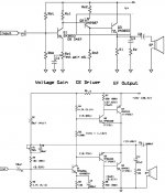
If you are interested in simple designs, here is another of mine. it was posted somewhere here a while ago but I couldn't find the link. the schematic is for a pre-amp and it can be redesigned to run as a power amp (I have done both). Essentially it is the half of the Nelson's latest Zen amp. Very good linearity, sweet sound, but hugely inefficient.
mashaffer said:Does that look like a workable design? I am not entirely sure about the stability of the bias currents.
I have built something similar:
http://www.diyaudio.com/forums/showthread.php?postid=359249#post359249
(in the thread of "simplest amplifier possible with BJTs")
Mine has considerable amount of feedback, primarily because of the non-linear nature of the 2nd / 3rd stage. I suspect that your will work but will have substantial amount of distortion. You may want to try it out in simulation first.
If you are interested in simple designs, here is another of mine. it was posted somewhere here a while ago but I couldn't find the link. the schematic is for a pre-amp and it can be redesigned to run as a power amp (I have done both). Essentially it is the half of the Nelson's latest Zen amp. Very good linearity, sweet sound, but hugely inefficient.
Attachments
Thanks millwood and destroyer
Millwood;
Thanks for the links. I will look them over. As for simulations I would love to be able to do that but as I am seriously unemployed I can't buy any software right now. Do you know of any freeware that a rookie like me could use to do this kind of simulation?
Destroyer;
Thanks. I wish I could take credit for the design but all I did was adapt it to 38V power supply. The class A thing I am trying to do from scratch.
Re: Thanks millwood and destroyer
Try Simetrix Intro (http://www.catena.uk.com/).
It's free, it's relatively easy to use and the device/node limitations are sufficiently generous to permit moderately sized analogue circuits to be simulated. The only downside is that it comes with a fairly small component model library, but models can be downloaded from many manufacturers' websites and they are easy to install (unlike some free simulation programmes).
mashaffer said:As for simulations I would love to be able to do that but as I am seriously unemployed I can't buy any software right now. Do you know of any freeware that a rookie like me could use to do this kind of simulation?
Try Simetrix Intro (http://www.catena.uk.com/).
It's free, it's relatively easy to use and the device/node limitations are sufficiently generous to permit moderately sized analogue circuits to be simulated. The only downside is that it comes with a fairly small component model library, but models can be downloaded from many manufacturers' websites and they are easy to install (unlike some free simulation programmes).
Thanks Geoff. I am going to download it as soon as I get the automatic email they send with the download instructions.
Thanks Millwood!!! That is really going the extra mile. This gives me a great starting point. When I get the Sim that Geoff recommended up and running I can use your results as a guide to whether I am modeling it properly. Once I have the basic model down then I can play with the circuit and see how good I can make the circuit without interstage FB. At that point I can decide whether to use additional feedback, howmuch and where.
Did you happen to notice during your run whether the circuit was getting enough gain to reach the full potential of the 15V PS and/or if there was any excess gain (could bypass less of the 1st stage emitter resistor in an attempt to improve THD)?
It might make sense for me to model the input stage by itself to see how much it contributes to the total distortion.
I sure hope I can get this sim software up. It could be a whole lot of fun and very educational.
Well time to go read up on amplifier distortion mechanisms.
mashaffer said:Thanks Geoff. I am going to download it as soon as I get the automatic email they send with the download instructions.
If you send me an email via the button below, or my website, I will send you the component model libraries that I have compiled over the past three years. They are mainly audio related components but it will be a start and will save you searching the manufacturer's websites, at least initially.
mashaffer said:Did you happen to notice during your run whether the circuit was getting enough gain to reach the full potential of the 15V PS and/or if there was any excess gain (could bypass less of the 1st stage emitter resistor in an attempt to improve THD)?
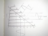
I didn't play with it much this time. But if you look at my chart, it is doing about 7-8vpp on the output. And distortion is very sensitive to the bias of the first stage: a couple of kohm out and you will immediately see distortion.
I sure hope I can get this sim software up. It could be a whole lot of fun and very educational.
you can get very good results with LTspice (at www.linear.com). It is also free and can be cutomized. You can also use ideal transistors and the result wouldn't be too far off.
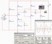
millwood said:well, I did it for you. Here is the simulation results from multisim.
I adjusted R1 to obtain the best output. THD pretty high, at 6%.
Try to add some small resistor between the emitter of the 2N3055, and the ground. It will set some local feedback, and increase the linearity.
sajti
- Status
- This old topic is closed. If you want to reopen this topic, contact a moderator using the "Report Post" button.
- Home
- Amplifiers
- Solid State
- New guy on the block thinking class A