Ok, I am happy to do so.
The system is complete monoblocks from mains to PSU to Power amp and is an 85 watt version of Geoff Moss's JLH configuration.
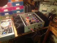
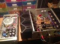
The first one is the separate PSU which contains a soft start circuit, 500VA transformer, bridge rectifier and initial smoothing. The case is an ex HP pulse generator case that I managed to get 3 of from FleaBay. There is then an unbilical cable to the Power amp case
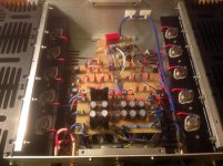
The second photo shows one half of the monoblock with the heat sink for the lower half of the output pair, plus the power transistor which is part of the negative rail capacitor multiplier, so that heat sink dissipates up to 150 watts (as does the other heat sink on the other side of the case) when the device is idle, you just see the other heat sink that has the upper part of the output pairs and the positive rail cap multiplier power transistor. The chunky red cable on the top of each power transistor is the connection to its Collector.
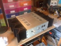
The third photo shows the whole device and the fourth the upper heat sink
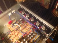
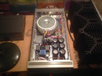
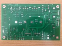
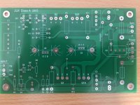
The next photo, if I have them in the right order, shows the layout of the cards.
Nearest is the dual rail cap multiplier with the secondary cap smoothing underneath.
Beyond that is the power transistor distribution board where all the output devices connect.
Lastly the card with the big red cap is the input and driver board - you can see the linking cable that carries the outputs to the upper and lower output pairs (white and purple cables) and takes the feedback from the output back to the driver (Grey cable)
What you cannot see if a small heat sink under the driver board that has the VAS and its current source transistor mounted on it.
The case is one of those Chinese cases off Ebay that I had to modify the metalwork of so as to get the heat sinks on - there is as almost as much work in the metal work as there is in the electronics")
The layout is where I took a lot of time on: I made the PCBs myself (except for the standard ones with the smoothing caps) as I enjoy doing that and wanted them made in a particular way. I then gold plated them to stop tarnishing. Earthing is very carefully done according to signal and smoothing etc. All crimps are crimped and soldered to get a really sound joint. (excuse the pun) and all the high current cable is 17 Amp rating.
The last photo is an older one of the amp with its lid on.
A lot of work but the end result is something that I am very pleased about, both construction and listening wise.
I hope it inspires you guys out there to go do
Cheers
Mike
The system is complete monoblocks from mains to PSU to Power amp and is an 85 watt version of Geoff Moss's JLH configuration.
The first one is the separate PSU which contains a soft start circuit, 500VA transformer, bridge rectifier and initial smoothing. The case is an ex HP pulse generator case that I managed to get 3 of from FleaBay. There is then an unbilical cable to the Power amp case
The second photo shows one half of the monoblock with the heat sink for the lower half of the output pair, plus the power transistor which is part of the negative rail capacitor multiplier, so that heat sink dissipates up to 150 watts (as does the other heat sink on the other side of the case) when the device is idle, you just see the other heat sink that has the upper part of the output pairs and the positive rail cap multiplier power transistor. The chunky red cable on the top of each power transistor is the connection to its Collector.
The third photo shows the whole device and the fourth the upper heat sink
The next photo, if I have them in the right order, shows the layout of the cards.
Nearest is the dual rail cap multiplier with the secondary cap smoothing underneath.
Beyond that is the power transistor distribution board where all the output devices connect.
Lastly the card with the big red cap is the input and driver board - you can see the linking cable that carries the outputs to the upper and lower output pairs (white and purple cables) and takes the feedback from the output back to the driver (Grey cable)
What you cannot see if a small heat sink under the driver board that has the VAS and its current source transistor mounted on it.
The case is one of those Chinese cases off Ebay that I had to modify the metalwork of so as to get the heat sinks on - there is as almost as much work in the metal work as there is in the electronics
The layout is where I took a lot of time on: I made the PCBs myself (except for the standard ones with the smoothing caps) as I enjoy doing that and wanted them made in a particular way. I then gold plated them to stop tarnishing. Earthing is very carefully done according to signal and smoothing etc. All crimps are crimped and soldered to get a really sound joint. (excuse the pun) and all the high current cable is 17 Amp rating.
The last photo is an older one of the amp with its lid on.
A lot of work but the end result is something that I am very pleased about, both construction and listening wise.
I hope it inspires you guys out there to go do
Cheers
Mike
Attachments


Last edited:
the photos seem to have gone west so here they are again.
I forgot to add even with that with all that heat sinking the temperature raises about 28 degrees C above ambient
Ooops photos reappeared
I forgot to add even with that with all that heat sinking the temperature raises about 28 degrees C above ambient
Ooops photos reappeared
Attachments


Last edited:
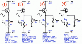
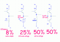
Class A has a theoretical efficiency of up to 50%. In practice, less. It is necessary to take into account the losses in the power source (transformer, rectifier, stabilizer, etc.).
A single-ended circuit with a resistor can be less than 10% efficient (Houston, Nelson Pass).
An amplifier topology like JLH2005 does not exclude the possibility of working in class AB when using darlington or mosfet.
Ideal:
Attachments
Last edited:
Mike!
Smart beautiful realization.
What about the stability of "0" at the output?
I am sorry I don't understand what you mean by that.
If you mean "Is it stable with the input shorted or open circuit" the answer is yes it is stable.
If you mean does the output D.C. offset vary much, the answer is 'No', the driver board has an adjustment for setting it up and it is within 10mV from cold to warm. What does vary is the quiescent current from cold to warm and this is about 200mA until thermal quiescence is reached.
Regards
Mike
Last edited:
I made my version of JLH 2005 some years ago.
I used what I had in hands... not too big heat sinks, an ancient 12+12Vac transformer, some TIP3055, and a BC560C as input transistor. No japanese trannies here. About 5 or 6 good watts for channel. 1A fuses at the outputs, dc output is stable at +-15mV. I made my own pcb layout, but I have a lot of troubles with hum and ground loops. I needed to cut some gnd traces in pcb amp, separating input to output stages, and making a star ground outside the pcbs...
Mine has a wood case, so a lot of heat from the heatsinks only.
Post your Solid State pics here.
It sounds good for me, with very detailed, relaxing sound. I can listen music for hours, it's not tiring to me at all.
Just because I could
I replaced the transformer in my 85 watt version for a 35 - 0 35, adjusted everything and got 104 watts from the design before clipping - rails of 42 volts, Iq of about 3.8 Amps or so.
Distortion was 0.05% before clipping although the higher harmonics were starting to appear at greater that 70 watts. At low powers, the distortion is down in the noise.
Regards
Mike
I had the PCBs made through Gerber's supplied by EUVL in post no 8, I am grateful
I do not understand
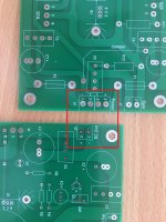
1- the output of power supply board and power supply input of driver board markings.DC out is 1 &2
DC input on driver board is 1,2 ,3, 4. ! corresponds to _ive on both boards, but 2 on power supply board is positive, does it go to No 4 on driver board?
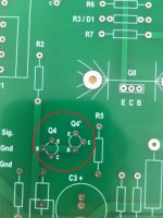
2- There is a white line next to Q1 on driver board, this supposed to be shorted ?
3- Looking at picture in post 1 , I am supposed to use "Q4'" position, one with ' ?
4- what is the specification of fuses.
5-I have two 500VA, 0-18v Toroidal Transformers and I intend to build mono blocks, is 18v enough or I need to purchase new transformers?
5-If some one responds I will next post the parts list and would appreciate if those in the know can say yes or no, please?
Thanks
Sajjad
I do not understand
1- the output of power supply board and power supply input of driver board markings.DC out is 1 &2
DC input on driver board is 1,2 ,3, 4. ! corresponds to _ive on both boards, but 2 on power supply board is positive, does it go to No 4 on driver board?
2- There is a white line next to Q1 on driver board, this supposed to be shorted ?
3- Looking at picture in post 1 , I am supposed to use "Q4'" position, one with ' ?
4- what is the specification of fuses.
5-I have two 500VA, 0-18v Toroidal Transformers and I intend to build mono blocks, is 18v enough or I need to purchase new transformers?
5-If some one responds I will next post the parts list and would appreciate if those in the know can say yes or no, please?
Thanks
Sajjad
Attachments
Last edited:
Since I did the PCBs, I shall only answer questions related to those.
They are 1:1 copies of those of Geoff, with no changes.
So not my design, but I try my best to answer.
You need two PSU board for one amplifier.
Each PSU board has only one polarity.
The amplifier has split rails, or 2 polarities.
The white line is a jumper.
Q4' is provided only to allow the use of alternative transistors with a different pin out.
You either populate Q4, or Q4', but not both.
Patrick
You should really read the website throughly before starting to build.
The Class-A Amplifier Site
Like your voltage question was already answered here :
The Class-A Amplifier Site - JLH Class-A Update
Patrick
The Class-A Amplifier Site
Like your voltage question was already answered here :
The Class-A Amplifier Site - JLH Class-A Update
Patrick
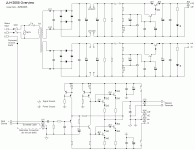
I am confused as original JLH had only + and - DC supply to the board and Geoff Moss version seems to have +/0/-
See enclosed picture from the "JLH-Class A Update" , have I got it correct that
To make one channel of amplifier, I need to build 2 power supply boards & combine the DC output of 2 power supply boards at driver board
d
See enclosed picture from the "JLH-Class A Update" , have I got it correct that
To make one channel of amplifier, I need to build 2 power supply boards & combine the DC output of 2 power supply boards at driver board
d
Attachments
- Home
- Amplifiers
- Solid State
- Geoff Moss's JLH-2005 design files