I did not notice that you added current feedback to the schematic in post #12.
That is not typically how feedback is done in differential amplifiers. Typically the VO+ feeds back to VI- and VO- feeds back to VO+ through feedback resistor Rf. Then an input resistor Ri is put in series with each input. Differential gain is -Rf/Ri, just like the inverting configuration of an op amp. The link shows an example.
Precision Fully Differential Op Amp Drives High Resolution ADCs at Low Power | Analog Devices
Your way should work, though. The advantage of your way is a very high impedance input.
I should warn you that you have a 3-stage amplifier, and you will need to stabilize so it does not oscillate with feedback. This is typically done with 100 pF or less from C to B of each Q2 and Q3. Do you know how to do Bode stability analysis?
openloop gain bodeplot
Hi Russel,
Yes I figured this feedback method was rather unconventional, however it looked sensible to me. Do you recommend another feedback method?
So far I have had one quarter of control theory. What I understand is that there where the openloop phase shift is -180 degrees, the openloop gain should be below 1. A teacher of mine recommended adding some C from C to B too. I see it creates a little high frequency lowpass through millers transformation.
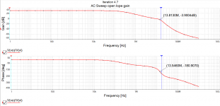
With the 10k feedback resistors removed and a Ccb of 22pF this is the openloop bodeplot I simulated is attached below. If I understand correctly, the system should be stable now.
According to this reasoning, it definitely was not stable before.
Recently watched Nelson Pass' final 2019 burning amp presentation where he claimed that emitter resistors at class AB output transistors result in slight compression. No emitter R however, would lead to the extension of dynamics.
Any thoughts on his claim? This definitely motivated me to try and live without emitter R.
Cheers and all the best,
Ruben
Hi Russel,
Yes I figured this feedback method was rather unconventional, however it looked sensible to me. Do you recommend another feedback method?
So far I have had one quarter of control theory. What I understand is that there where the openloop phase shift is -180 degrees, the openloop gain should be below 1. A teacher of mine recommended adding some C from C to B too. I see it creates a little high frequency lowpass through millers transformation.
With the 10k feedback resistors removed and a Ccb of 22pF this is the openloop bodeplot I simulated is attached below. If I understand correctly, the system should be stable now.
According to this reasoning, it definitely was not stable before.
Recently watched Nelson Pass' final 2019 burning amp presentation where he claimed that emitter resistors at class AB output transistors result in slight compression. No emitter R however, would lead to the extension of dynamics.
Any thoughts on his claim? This definitely motivated me to try and live without emitter R.
Cheers and all the best,
Ruben
Attachments
I think Nelson pass is wrong on that one. There are two optimum bias points. One is class A, where the output impedance is 1/(2 gm) all the time. The other is optimum class B where the output impedance is 1/gm all the time.
People find that biasing with the voltage on the emitter resistors at around 26mV to be optimum.
On your plot, you can compensate more. There is no harm in your -3dB point being at 20 kHz.
People find that biasing with the voltage on the emitter resistors at around 26mV to be optimum.
On your plot, you can compensate more. There is no harm in your -3dB point being at 20 kHz.
There a tons of threads on diyaudio devoted to optimum class-B bias. This one is short and to the point. Apparently some guy at Hewlett Packard did some math in the 1960s and determined the 26 mV number. It's a little more complicated than that. Many people find that
- The optimum class B bias point is with voltage across the RE somewhat less than 26 mV. Usually in the 15 to 20 mV range.
- People listening find that simply more bias is better, because at low listening levels, the output is class A. And at higher listening levels, distortion is less audible. Most important is how much THD the amp has at low signal levels.
This may be one of the oldest threads about optimum class-B bias here:
"Optimum" Class B better than Class AB?
"Optimum" Class B better than Class AB?
So far I only used Gm with JFets. Not sure how to find it for bjt's.
I absolutely agree that THD is most critical till say 1 to 2 watts. So we want to stay in class A with Zout at 1/2gm untill we surpass some point and go class B with Zout at 1/gm. As Zout goes up with larger signals, slight compression should occur right?
I can increase the current through the biasing transistors (Q15, Q17) or increase their Re to get more class A. When I add Re's to the output (Q23, Q25) the amp goes class B sooner. How does this work?
Cheers,
Ruben
Attachments
For BJT's gm = Ic/Vt, where Vt is the thermal voltage kq/T, with T in Kelvin. With T=300 (27deg Celsius), Vt=26mV.
So gm = Ic/26mV. With a BJT running 1mA, gm = 38.5 mill-mhos. The input resistance of a CE BJT with no emitter is Rpi or hie, depending on your undergrad textbook. Rpi=beta/gm.
When you add RE, you have to increase the bias voltage to account for the additional voltage drop of IE*RE. So, after adding RE, increase the bias until the current is the same as it was previously.
In the scenario you describe, as you transition out of class-A operation, the gain would decrease, and there would be some compression. This is nothing to do with having an RE.
Adding an RE gives the stage a new effective Gm = 1/(beta(1/gm+RE)). Some people write it as 1/(Rpi + (beta+1)RE). The equations are about equal if beta >> 1.
The Gm that doubles as you transition into class A operation is this new effective Gm. You may have noticed that little gm (not including the RE) is proportional to current. Adding the RE linearizes that gm a bit. Maybe this is what Mr. Pass means by RE compressing the signal. Without RE, the signal is being expanded by ever-increasing gm as output current increases. With RE, the expansion is less. Is less non-linear expansion equal to compression? I guess that depends on your perspective. In a single-ended output, which Mr. Pass likes, that expansion gives 2nd harmonics. In a push-pull, those 2nd harmonics are mostly cancelled, leaving only the odd-order harmonics to dominate. That, in a nutshell is why Nelson Pass likes single-ended output topology.
This is an over-simplification, based on only looking at gm. In actual output stages, beta degrades at high current, loading the VAS ever harder as current increases. The net result is almost always less voltage gain through the output stage at high current. Looking at gm alone would lead you to expect the opposite.
Last edited:
Hi Ruben,Hi Russel, ...
Recently watched Nelson Pass' final 2019 burning amp presentation where he claimed that emitter resistors at class AB output transistors result in slight compression. No emitter R however, would lead to the extension of dynamics.
Any thoughts on his claim? This definitely motivated me to try and live without emitter R.
Ruben
I'm not Russell but I followed Nelson's BAF2019 talk on source resistors and squarelaws see post Square Law Amp
it shows source resistors in amps are bad news and best avoided when possible.
But for BJT amps some emitter resistance is essential to stop thermal runaway. Use Bob Cordell's book equation 15.6 (1st Ed) to stop thermal runaway: Gmax=1/(2.2mV/C*Vrail*1.6C/W) where Vrail is for split supplies (Vcc/2 for your amp). 1.6C/W is for a TO-247 0.83C/W and 0.8C/W washer. With Vcc=35V Gmax=16.7A/V. This is per transistor. At idle both halves have equal gains so the total Gm max is 33.4A/V. So the emitter resistance must be more than 30m Ohms for this amp. Applying a safety factor of 2 you need at least 60m Ohms. Since the power transistors have some internal series resistance (maybe 30m Ohms see here) you need to add say 33m Ohms minimum. If say you increased the supply voltage by 50% then the minimum resistance goes to 90m Ohms total or 68m Ohms external. If your thermal washers are 50% higher then you need 75m Ohms or 47m Ohms external. Etc.
But for most amps with split rails the minimum emitter resistance must be doubled because the transistors have twice the voltage across them to generate twice the heat at idle. For a split rail amp with +/-35V rails the minimum emitter resistance is 60 m Ohms or 120m Ohms with the safety factor of 2 so 100m Ohms external. If the supply voltage was say +/-50V then use 150m Ohms minimum. Etc.
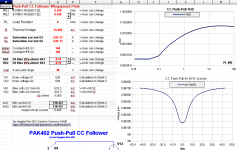
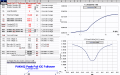
The effect of different emitter resistances on the distortion can be downloaded for a Class-AB follower from my website PAK2 2021 updates - PAK2 devo
Here are 2 examples with emitter resistances of 100m Ohms and 56m Ohms (total R):
.
.
The THD values here are fairly close to LTspice for the exact same transistors etc so good enough to see general trends. They are for the follower output stage only so no global feedback is used here at all. The transistor model is as a pure exponential and at low frequency with no other nonidealities like Early effect or Beta fall at high current, or the driver stage, etc. It is intended to show the upper limit of performance from an output stage and how the emitter resistance (and Re mismatch and Beta mismatch) affects the performance from first principals.
One interesting thing it shows is that 100m Ohms emitter resistance can get the THD below 0.03% for most of the power range. I found from listening tests that a THD of 0.03% or less was not audible to my ears under the very best of listening conditions (as published in Linear Audio Vol.4). So I'd be happy to not use any global feedback for an amp with 100m Ohms or less. But not with 200m Ohms which is a more common value these days with THD figure usually aiming for 0.003% or less.
Attachments
Hi Ian,
whoever you are im happy to receive your input. Its good to read your extensive story. As of now i am using NI multisim only and im hitting a brick wall. I should try TLspice, hopefully it allows me to do more than just sweeps.
Currently using 56m ohm Re's. Indeed yields nice results. Thank you for the sources you shared. Will dive into them at some point.
Cheers,
Ruben
Phase shift at 20k
Hi All,
Quick question: How much phase shift is too much? The amplifier needs a capacitor from collector to base at the voltage gain stage to ensure stability, however it brings a phase shift of 2.2 degrees with it at 20k.
Can I just introduce some series inductance in the feedback loop to counter this phase shift? This way closed loop gain should increase slightly at high frequencies while open loop gain remains untouched.
Though I can't confirm with experience, I understood human ears are quite sensitive to phase shift. What do you think?
Cheers,
Ruben
I would not worry about this.
The human ear is actually almost completely insensitive to phase shift. Very few human ears can hear 20 kHz at all, and none can hear the phase shift at 20 kHz. Experiments were done with all pass filters that introduced phase shift in the midrange, but not amplitude change, and no one could hear it at all.
The cochlea in your ear is progressive filter (a spiral), with auditory nerve endings along the way. Each nerve ending senses a band of frequencies. The nerve senses if a frequency is present, but not its phase. The brain does a lot of post-processing on the incoming sound, but it's not fast enough to sort timing differences below about 15 ms.
True differential or dual SE in balanced operation?
Hi All,
A teacher of mine recommended using a more conventional layout: A diffpair followed by a single VAS and a single output buffer and using NFB like all the blameless amps out there. Since I wanted bridged ins and outs from the start, it will be operating as Dual SE balanced: (which would also be a diff amp)

This actually resembles how the design started life, but since the diffpair already gives us a differential output, I though it was quite cumbersome to use two for one channel. Once I got it to work with just one diffpair as a true differential amplifier I was sold.
However going for the conventional design and its NFB method, we get unity DC gain and the desired AC gain making extra op-amp for common mode feedback redundant. So I gave it another try. The result yields quite similar performance from what I can tell. Only the Dual SE version needs more capacitance (in feedback and Ccb) and as a result there quite a lot more phase shift at very low and high frequencies (up to 10 degrees), something I once thought I had to avoid.
Meanwhile at the true differential version: I added current sources to the emitters of the pnp VAS. So far I couldn't get it to work with current sources at the collectors or with the (pre output) driver and voltage stages swapped:

I am looking for a more sophisticated VAS solution. Maybe a voltage stage diffpair or something like shown in the third attachment.
Both versions can output a decent 20Vrms, 5Arms into 4 ohm at about 55 percent efficiency. Av for both is 15. The dual SE version would need an extra dual jfet, which isn't cheap. Which do you recommend? I'm in dubio.
All thoughts and opinions are welcome.
Cheers,
Ruben
Hi All,
A teacher of mine recommended using a more conventional layout: A diffpair followed by a single VAS and a single output buffer and using NFB like all the blameless amps out there. Since I wanted bridged ins and outs from the start, it will be operating as Dual SE balanced: (which would also be a diff amp)
This actually resembles how the design started life, but since the diffpair already gives us a differential output, I though it was quite cumbersome to use two for one channel. Once I got it to work with just one diffpair as a true differential amplifier I was sold.
However going for the conventional design and its NFB method, we get unity DC gain and the desired AC gain making extra op-amp for common mode feedback redundant. So I gave it another try. The result yields quite similar performance from what I can tell. Only the Dual SE version needs more capacitance (in feedback and Ccb) and as a result there quite a lot more phase shift at very low and high frequencies (up to 10 degrees), something I once thought I had to avoid.
Meanwhile at the true differential version: I added current sources to the emitters of the pnp VAS. So far I couldn't get it to work with current sources at the collectors or with the (pre output) driver and voltage stages swapped:
I am looking for a more sophisticated VAS solution. Maybe a voltage stage diffpair or something like shown in the third attachment.
Both versions can output a decent 20Vrms, 5Arms into 4 ohm at about 55 percent efficiency. Av for both is 15. The dual SE version would need an extra dual jfet, which isn't cheap. Which do you recommend? I'm in dubio.
All thoughts and opinions are welcome.
Cheers,
Ruben
Attachments
I have a lot to unpack here, so I'm doing it in 3 posts.
There are pros and cons to what your teacher is saying. If you know you are going to bridge it, and never use it single ended, then the fully differential amp is the correct approach. If you think you might like the flexibility of a stereo amp with 2 by X watts, or a mono bridged amp with 1 x 4X watts, then you want to do 2 SE amps. One is non-inverting and the other is inverting. If you flip the speaker leads on the inverting amp, it corrects the polarity.
Weren't you thinking of doing three of these bridged beasties? If you do them all SE, then you can have 6-channel, 4.1 or 2.1. You only need a Y-connector on a pair of inputs to choose mono-bridged for that pair. Up to you.
A teacher of mine recommended using a more conventional layout: A diffpair followed by a single VAS and a single output buffer and using NFB like all the blameless amps out there. Since I wanted bridged ins and outs from the start, it will be operating as Dual SE balanced: (which would also be a diff amp)
View attachment 935135
There are pros and cons to what your teacher is saying. If you know you are going to bridge it, and never use it single ended, then the fully differential amp is the correct approach. If you think you might like the flexibility of a stereo amp with 2 by X watts, or a mono bridged amp with 1 x 4X watts, then you want to do 2 SE amps. One is non-inverting and the other is inverting. If you flip the speaker leads on the inverting amp, it corrects the polarity.
Weren't you thinking of doing three of these bridged beasties? If you do them all SE, then you can have 6-channel, 4.1 or 2.1. You only need a Y-connector on a pair of inputs to choose mono-bridged for that pair. Up to you.
OK, don't put current sources in the emitters of the VAS. Putting current sources in the emitters, you have just killed all the gain of the VAS common-emitter stage. The gain of the VAS is approximately -Rc/Re. You have changed out Re=56 ohm for Re ~= (beta*56 ohms).Meanwhile at the true differential version: I added current sources to the emitters of the pnp VAS. So far I couldn't get it to work with current sources at the collectors or with the (pre output) driver and voltage stages swapped:
View attachment 935136
A current source at the collector of the VAS will replace the 3.9K resistor with the output impedance of the current source. Probably 50 to 100 times higher, depending on the current source. Your gain would go up by 50 times or more. You probably could not make it work because the amp became unstable with all this extra gain. You have to increase the value of C1 and C2 to stabilize it.
If you put the pre-driver buffer before the VAS, it has to be a PNP buffer. Sorry I did not tell you that. The CM feedback will increase the current in R1 and R2 for the extra Vbe drop. Or you can increase R1 and R2 to keep the current the same. You also have to connect the compensation caps C1 and C2 across to the buffer inputs for the compensation to work.
Even better is to have an emitter-follower buffer both before and after the VAS.
I am looking for a more sophisticated VAS solution. Maybe a voltage stage diffpair or something like shown in the third attachment.
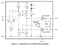
Well, now this is something very different. This is a differential folded-cascode stage with proper common-mode feedback. Actually, this is a dual-ended version of my RK-autobias-200W amplifier.
The CM feedback is exactly what I was describing in post 13.
There are pros and cons to what your teacher is saying.
Weren't you thinking of doing three of these bridged beasties?
Haha if at some point i'm totally convinced this design is worth it, I will build two of these bridged beasties. Definitely not gonna use SE. AC line is dirty AF here, through my current SE amp i can hear my refrigerator switch on and off. Don't have another group available. And I just love the bridged concept.
My teacher warned me that the DC servo can add a lot of distortion, this is why he thinks regular NFB is better opposed to CFB. I'm not sure if he had more reasons next to modularity.
Driver VAS sandwich it is then. Of source it has to be PNP, common sense should've been enough to realize this. Thanks for the tips Russel! The VAS performs much better now.If you put the pre-driver buffer before the VAS, it has to be a PNP buffer. Sorry I did not tell you that. The CM feedback will increase the current in R1 and R2 for the extra Vbe drop. Or you can increase R1 and R2 to keep the current the same. You also have to connect the compensation caps C1 and C2 across to the buffer inputs for the compensation to work.
Even better is to have an emitter-follower buffer both before and after the VAS.
- Home
- Amplifiers
- Solid State
- Class AB diff-amp design