I simply reverse the labels on the right channel speaker terminals to fix the polarity. Doing this has two benefits: 1) the amp automatically bridges to mono by using the L+ and R- terminals. 2) the two channels draw their currents from the opposite supply rails, reducing voltage sag on the rails and cutting in half the peak current in the rectifiers.
Aargh...
Why not add one differential stage and one output stage for each channel and make each channel fully balanced?
A couple of volts common-mode will change the 4 mA tail current by less than 4uA.
Now convert those in dB and you'll catch my idea.
The KSA1381 cascode devices are no less linear than a CE VAS stage with similar output impedance.
Heh. Your VAS have two shoulders loaded on the current mirror. One shoulder under full rail-to-rail voltage while second at idle have only half of such a voltage, one rail (for zero at the output. Just add one ground-referenced cascode device to a left shoulder and you'll round that voltages at the main zero crossover point.
The main source of distortion in BJT amplifiers is dependency of small-signal parameters on collector current.
No.
Main (measurable) distortion effect is a collector current dependance of collector-emitter voltage at the huge voltage swing point. I.e. Early effect at the VAS output high-impedance node. Yes, this distortion exists even at truly constant current-source load and dominates even being compared with known OPS distortion.
Just add one ground-referenced cascode device to a left shoulder and you'll round that voltages at the main zero crossover point.
Like this:

Last edited:
Aargh...
Why not add one differential stage and one output stage for each channel and make each channel fully balanced?
Like this:

Aargh...
Why not add one differential stage and one output stage for each channel and make each channel fully balanced?
I could, and get lower distortion with cancellation of even harmonics. But I don't like the cancellation of even harmonics. Also, I'm using enough transistors already. I've designed a fair number of fully differential amps in my life, including a 20 GHz GBW amp with switched-cap CM feedback in 16nm CMOS. I don't see fully differential as the correct solution for audio power amps.
Now convert those in dB and you'll catch my idea.
Sure. That's -60dB of common mode signal. The differential to single-ended conversion by the mirror in the next stage nulls the delta I by another 40dB, at least. Global feedback reduces that by another 74 to 50 dB, depending on the frequency. That's a 150 to 174 dB of immunity to common-mode voltage of the closed-loop amplifier. Immeasurable and inaudible.
If you look in post #38, I cascoded the tail current, which brought the delta-Ic down by another 40 dB and that had no affect on distortion.
Heh. Your VAS have two shoulders loaded on the current mirror. One shoulder under full rail-to-rail voltage while second at idle have only half of such a voltage, one rail (for zero at the output. Just add one ground-referenced cascode device to a left shoulder and you'll round that voltages at the main zero crossover point.
I already did this. You should read the whole thread. Look at post #8 where jcarr suggested the same, followed by some discussion in the next few posts, and then in post #15, where I added Q30. It really only affects offset voltage and heating of Q5. Not THD.
No.
Main (measurable) distortion effect is a collector current dependance of collector-emitter voltage at the huge voltage swing point. I.e. Early effect at the VAS output high-impedance node. Yes, this distortion exists even at truly constant current-source load and dominates even being compared with known OPS distortion.
None of those statements are correct, and they are especially incorrect for cascoded VAS stages. Early voltage is not the dominant distortion mechanism, even without cascoding. Cascoding multiplies the Early voltage by beta of the cascode device. Voltage swing effects the gain of the stage if it causes the collector current to change. For a folded cascode, that effect is negligible. I explained all this in detail in post #36.
In any CE gain stage, the main nonlinearity is the Ebers-Moll equation, shown. Early voltage and Cbc are much lower order. Ebers-Moll is the same for every transistor, but Early voltage and Cbc vary greatly. So I can see why you think they are the main distortion mechanisms. Because they are what change when you swap transistors.
Attachments
Last edited:
Mr. Self has another thing very right: if the dominant source of distortion is the input pair, then emitter degeneration is the cure. Loss of low frequency loop gain is offset by the addition of local feedback. The compensation cap can then made smaller to bring high frequency loop gain back to the original level. This further increases input pair linearity at high frequency, because they are not having to slew as hard to charge the compensation cap.Doug Self, on page 228 of his 6th edition amplifier design book, says (paraphrase) that he doesn't know much about designing folded cascode amps, but he does have one thing right. There is no Miller compensation, not even Miller Input Compensation.
I'm tabling that for now, because I'm currently working on SOA protection.
Chapter 24 of Doug Self's Audio Power Amplifier Design has a nice overview of current limit and SOA schemes. That is great, because that has always been my weak spot as an amp designer.It's time to put in protection circuits, output coil, bypass caps, and layout the PCB.
To get the output current to limit, the SOA protection has to pull 4.4mA from the collector of Q8 (or add 4.4 mA to Q9).The FC quiescent current (Q8) is 2.44 mA with a 12uA pkpk swing, when driving 8 ohms to 200W. If the SOA circuit pulls 6uA, distortion will at least double.
If the SOA circuit limits current to 24A, then at 18 A, the OC protect is already doubling distortion, and will noticeably affect linearity at 16 A or less. 16 A is close to peak current for a 4 ohm load. There seems to be a possibility of the protect circuit adding THD to normal operation.
The SOA circuits use a transistor to sense the voltage across a ballast resistor, so the limit is not at all precise. It occurs to me that I have a sense resistor and precision current sense circuit already hanging from each supply rail. Instead of a transistor, I can use a precision reference (back to the TL431 again) to push or pull current from the FC stage. It would basically have no effect at all on the FC stage until the SOA current limit is met, and then it would pull the full 4.4 mA right away. The last challenge is to make sure the limit circuit doesn't oscillate.
The attached pics are my SOA circuit experiment (single slope) and the plot of the SOA limit alongside the Pdiss limits of the transistors (MJL0281 and MJW3281) and the 2 ohm, 4 ohm, and 8 ohm load lines.
Attachments
Last edited:
Limitations of LTspice
I tried the SOA circuit I drew in the previous post. I had to tweak it to get the SOA limit line I wanted, but that was expected. I was right that the limit circuits would affect THD. I drew current from the collectors of cascodes Q8 and Q10.
At 100 Hz
Then I realized that because I flipped my first EF stage upside down, I could steal the current from its constant current sources. That location is a lot less sensitive to a few uA of current injection.
That's much better, but the last two are still quite bad. Ironically, I was proud of amps I built 25 years ago with 0.02% THD. I had to set the limits to far outside the SOA to get the THD back down. Also, LTspice was starting to get fairly cranking about convergence with SOA limiters installed in the amp.
I then tried the SOA limiters you see in the attached circuit. I'd like to report that these worked great, but I ran hard into the limits of LTspice. This circuit simulation won't converge no matter what I try.
I did run a simulation of just the limiter circuit to see if it gave me my predicted SOA line. It did. No tweaking required. I would just like to know if the TL431 version causes additional THD. That experiment will have to wait for circuit boards, and I will need a plan B, such as a relay on the speaker terminal if the SOA limiter trips. I had hoped to avoid that.
[RANT]
I am accustomed to doing "whole IC" mixed signal simulations of ADC circuits, where the IC has thousand of transistors, lots of non-linear functions with sharp edges, and millions of extracted layout parasitic R and C elements. The signal is 10 MHz, the sampling frequency is 100 MHz, and the internal clock is 2.5 GHz. I have pored over terabyte spice result files. It may take a while to run (days in fact), but it almost always converges.
[/RANT]
I should not complain. LTspice is very good for what I paid for it.
I tried the SOA circuit I drew in the previous post. I had to tweak it to get the SOA limit line I wanted, but that was expected. I was right that the limit circuits would affect THD. I drew current from the collectors of cascodes Q8 and Q10.
At 100 Hz
Code:
PWR   THD-no SOA  THD-SOA
1W    0.000064%   0.000069%
10W   0.000178%   0.00313%
100W  0.000452%   0.0365%
200W  0.000640%   0.536%   <--horrible!
Then I realized that because I flipped my first EF stage upside down, I could steal the current from its constant current sources. That location is a lot less sensitive to a few uA of current injection.
Code:
PWR   THD-no SOA  THD-SOA
1W    0.000064%   0.000069%
10W   0.000178%   0.000226%
100W  0.000452%   0.0296%
200W  0.000640%   0.0205%
That's much better, but the last two are still quite bad. Ironically, I was proud of amps I built 25 years ago with 0.02% THD. I had to set the limits to far outside the SOA to get the THD back down. Also, LTspice was starting to get fairly cranking about convergence with SOA limiters installed in the amp.
I then tried the SOA limiters you see in the attached circuit. I'd like to report that these worked great, but I ran hard into the limits of LTspice. This circuit simulation won't converge no matter what I try.
I did run a simulation of just the limiter circuit to see if it gave me my predicted SOA line. It did. No tweaking required. I would just like to know if the TL431 version causes additional THD. That experiment will have to wait for circuit boards, and I will need a plan B, such as a relay on the speaker terminal if the SOA limiter trips. I had hoped to avoid that.
[RANT]
I am accustomed to doing "whole IC" mixed signal simulations of ADC circuits, where the IC has thousand of transistors, lots of non-linear functions with sharp edges, and millions of extracted layout parasitic R and C elements. The signal is 10 MHz, the sampling frequency is 100 MHz, and the internal clock is 2.5 GHz. I have pored over terabyte spice result files. It may take a while to run (days in fact), but it almost always converges.
[/RANT]
I should not complain. LTspice is very good for what I paid for it.
Attachments
Last edited:
I just remembered there's a 1.2V version of the TL431, the TLV431. That's clearly a much better IC for the SOA application. Spanning across 2 EF stages provides plenty of headroom for the TLV431, but not for the TL431. Even 3 EF stages is too small a voltage for a TL431. That's why I added 2 diodes below where U2 connects to Q11.
Swap out U2 with a TLV431 and reduce R102 from 165 to 82.5 ohms
Swap out U4 with a TLV431, reduce R104 from 332 to 165 ohms, and R105 to 174.
Now if only someone would make a PNP version of the TLV431.
Oh, wait, I need to cascode U4 for voltage protection.
Swap out U2 with a TLV431 and reduce R102 from 165 to 82.5 ohms
Swap out U4 with a TLV431, reduce R104 from 332 to 165 ohms, and R105 to 174.
Now if only someone would make a PNP version of the TLV431.
Oh, wait, I need to cascode U4 for voltage protection.
Solving SOA Protection
My goal with SOA protection is no relay and no added distortion when driving normal 8 ohm and 4 ohm loads. I tried the SOA circuits in Doug Self's amplifier book and they definitely increase distortion. Bipolar transistors turn on too gradually. One decade of Ic change per 60 mV of Vbe change starts at a surprisingly low Ic. Setting the SOA protection line below the SOA curve of the output transistor resulted in THD leaping to over 0.5% from 0.0006% without SOA limiting.
My thought was to try IC shunt regulators in place of the BJTs. I had a circuit that could work if I could stabilize it. The gain of the IC regulators is so high, that I could not stabilize the current-limit loop.
So, I went back to the BJT sense transistor, but now with a 1.2 V shunt regulator in series with the emitter. This connection still allows the lower gain and stability of the BJT sense, but gives and additional 1.2V before the sense transistor starts to flow current. This actually does the trick.
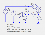
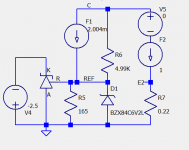
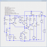
A test circuit is shown for the PNP side of the output stage. The NPN side is complementary. Current is sensed on the 0.1 ohm resistor, modeled by V5 here, and divided by 10,000, modeled by F1. That current is pulled through R1 and turns on Q5 when the limit is reached. R2 serves to lower the current limit when Vce is high. Q5 and Q2 subtract from the constant Q3 current. When there is no current left for Q4, output current is maxed.
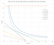
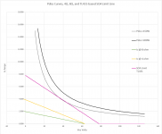
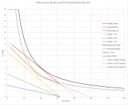
In Excel, I plotted the SOA line of the limit circuit on the SOA curves of the transistors. (This is really the same Pdiss and load lines as in post #66, but on a log/log chart.) Only the SOA protection line is new data. For the curves, I disconnected C1, so there's no time-weighting. The solid blue is the data from the simulation stepping Rload from 0.1 to 2 ohms. The dotted line is Excel extending the linear function to the axes.
When I run with 4 and 8 ohm loads, Q5 current remains below 10 nA, which is insignificant.
A final comment: With the first EF stage in a diamond configuration, I am able to current limit at this stage, rather than the VAS. The VAS is very sensitive to anything you attach to it, so this is good. Attaching to the EF stage reduces audible artifacts from the limit transistor by the factor of beta of the EF transistor.
Then I ran sims with 8 ohm and 4 ohm loads. Q5 current remained below 10 nA
My goal with SOA protection is no relay and no added distortion when driving normal 8 ohm and 4 ohm loads. I tried the SOA circuits in Doug Self's amplifier book and they definitely increase distortion. Bipolar transistors turn on too gradually. One decade of Ic change per 60 mV of Vbe change starts at a surprisingly low Ic. Setting the SOA protection line below the SOA curve of the output transistor resulted in THD leaping to over 0.5% from 0.0006% without SOA limiting.
My thought was to try IC shunt regulators in place of the BJTs. I had a circuit that could work if I could stabilize it. The gain of the IC regulators is so high, that I could not stabilize the current-limit loop.
So, I went back to the BJT sense transistor, but now with a 1.2 V shunt regulator in series with the emitter. This connection still allows the lower gain and stability of the BJT sense, but gives and additional 1.2V before the sense transistor starts to flow current. This actually does the trick.
A test circuit is shown for the PNP side of the output stage. The NPN side is complementary. Current is sensed on the 0.1 ohm resistor, modeled by V5 here, and divided by 10,000, modeled by F1. That current is pulled through R1 and turns on Q5 when the limit is reached. R2 serves to lower the current limit when Vce is high. Q5 and Q2 subtract from the constant Q3 current. When there is no current left for Q4, output current is maxed.
In Excel, I plotted the SOA line of the limit circuit on the SOA curves of the transistors. (This is really the same Pdiss and load lines as in post #66, but on a log/log chart.) Only the SOA protection line is new data. For the curves, I disconnected C1, so there's no time-weighting. The solid blue is the data from the simulation stepping Rload from 0.1 to 2 ohms. The dotted line is Excel extending the linear function to the axes.
When I run with 4 and 8 ohm loads, Q5 current remains below 10 nA, which is insignificant.
A final comment: With the first EF stage in a diamond configuration, I am able to current limit at this stage, rather than the VAS. The VAS is very sensitive to anything you attach to it, so this is good. Attaching to the EF stage reduces audible artifacts from the limit transistor by the factor of beta of the EF transistor.
Then I ran sims with 8 ohm and 4 ohm loads. Q5 current remained below 10 nA
Attachments
That's a good paper. I read it about 2 weeks ago, as I started grappling with SOA limiting.
It puts the math to several of the circuits that Doug Self put in his book, and shows the principles of how they give multiple slopes. The protection of my amplifier may end up being dual slope, in order to deal with reactive loads. I still need to do some simulation to determine what it will need. Triple slope certainly seems unnecessary.
Kiwanuka doesn't go far enough to address the problem of gradual turn-on that is inherent to a simple transistor sensor. Transistors turn on too gradually for me to use them as sensors without raising the threshold voltage at which they start to conduct.
In post #67 I showed how the barely adequate single-slope protection in post #66 destroys the high power THD performance of the amplifier. Increasing the number of slopes will not address this basic flaw in the exponential relationship of Ic to Vbe. The sense transistor starts working far earlier than it should. I tried sharp-threshold shunt regulators, but they have too much gain, and create feedback loops that are very difficult to stabilize.
Now I have the basic building block of a transistor with a 1.2V shunt regulator in its emitter--it has very little leakage until > 1.2V, and then has low gain as it begins to operate, I can implement whatever multi-slope SOA I need to give me the headroom for reactive loads, knowing that it will not affect THD at normal 8 and 4 ohm operation.
Mirroring the current from the rails instead of sensing on a ballast resistor is also key to my technique. Sensing the voltage across a ballast resistor, I could not find a technique that caused the sense transistor to have super-low current below the SOA limit. I need the sense transistor current to be at least 3 decades lower than at the threshold point, or around 500 nA, in order to not degrade the linearity much. That means a Vbe 200mV below the 650mV at threshold. At around 70% of the SOA limit, THD is begins to degrade.
If I were feeding back to the VAS, I would need it another 2 decades lower. The standard method, regardless of the number of slopes, begins affecting the linearity at just over 1/2 the limit threshold.
Putting a diode in series with the sense node helps, but not enough. Turn on is still too gradual. In the same way, in my scheme, just putting a diode or two in series with the base or emitter would help, but not enough. The sharp threshold of a IC bandgap reference is just what I needed.
Turn on is still too gradual.
Use one more bjt as emitter follower. It will help to make the turn on much sharper.
Sajti
Thanks for the tip, Sajti, but I already have this problem solved to my satisfaction, as shown in post #70. I'm going to add a 2nd slope to the SOA to extend the amp to higher VCE operation. Here are my next steps:
1) Run some reactive load sims to see what I can expect from a 4 ohm speaker with a high Q and a difficult crossover.
2) Calculate the resistors and diodes I need for a 2-slope SOA that powers that speaker without distortion.
1) Run some reactive load sims to see what I can expect from a 4 ohm speaker with a high Q and a difficult crossover.
2) Calculate the resistors and diodes I need for a 2-slope SOA that powers that speaker without distortion.
Also, LTspice was starting to get fairly cranking about convergence with SOA limiters installed in the amp.
I then tried the SOA limiters you see in the attached circuit. I'd like to report that these worked great, but I ran hard into the limits of LTspice. This circuit simulation won't converge no matter what I try.
Did you try the alternate solver setting in the preferences?
Hi Jaycee,
Thanks. I tried that and reltol, Gmin, abstol, and Trtol.
Generally, if I'm on normal, I switch to alternate, and vice versa. Then I move reltol from 0.001 to 0.003. Then Gmin to 1e-10. Then abstol to 1e-10. Then I change Trtol from 1 to 7 or from 7 to 1, or sometimes 4 or 5. If it's still not working I relax Gmin, abstol, and Trtol even further.
Sometimes, tweaking on these settings makes it work, and sometimes putting them back is what works. Often, nothing works, no matter what I try. LTspice loves it when your circuit has mostly linear, or only gradual nonlinearities. Diode junctions and FETs are fine, mostly. LTspice hates it when you have sharp non-linearities, like with IC regulators and references, when they are inside a feedback loop.
LTspice is supposed to be oriented to switchmode power supply simulations, but given its difficulty with IC voltage references, I don't see how. I'd love to be able to use Cadence's Spectre simulator, HSpice, or even Texas Instrument's internal TI-Spice (not TINA). These simulators are brutally accurate (actually it's the models) and heroic convergence on huge circuits.
I'm on LTspice's groups.io list. They often have models there for various devices, and some tips for getting it all to work.
I have added dual-slope to the SOA limiit circuit in post #70.
V5 and F1 are a quick model for a current sense circuit. V5 represents a 0.1 ohm resistor, and F1 represents an op amp + NPN current mirror that divides the current in the 0.1 ohm resistor by 10,000.
R1 sets the current limit when Vce=0V.
R2+R11 sets the limit when Vce is between 0 and 37V.
The ratio of R2 and R11 and the 15V zener voltage sets the 37V threshold.
R10 and zener diode D1 move the SOA limit line to a shallower slope when Vce > 37V.
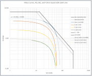
This was simulated by stepping R3 (the speaker load) and sweeping VIN at each step from 0 to 60V.
Next I will determine a C value to go in parallel with R1 for time-weighting the SOA. Probably about 33uF. Then I add this to the big schematic. This will go on a daughter PCB that also includes the bias servo.
V5 and F1 are a quick model for a current sense circuit. V5 represents a 0.1 ohm resistor, and F1 represents an op amp + NPN current mirror that divides the current in the 0.1 ohm resistor by 10,000.
R1 sets the current limit when Vce=0V.
R2+R11 sets the limit when Vce is between 0 and 37V.
The ratio of R2 and R11 and the 15V zener voltage sets the 37V threshold.
R10 and zener diode D1 move the SOA limit line to a shallower slope when Vce > 37V.
This was simulated by stepping R3 (the speaker load) and sweeping VIN at each step from 0 to 60V.
Next I will determine a C value to go in parallel with R1 for time-weighting the SOA. Probably about 33uF. Then I add this to the big schematic. This will go on a daughter PCB that also includes the bias servo.
Attachments
Did you try the alternate solver setting in the preferences?
I found the magic option in this particular circuit to make it run almost every time.
.options cshunt 0.1p
That basically adds 0.1pF from every node to GND. I would not add that to every circuit sim, but it helped this one converge, and is probably not too far from real world parasitic. 2 parallel metal strips in a proto-board have about 3 pF between them.
Attachments

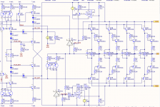
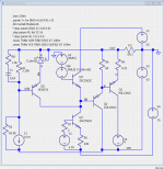
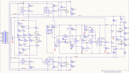
I've drawn the schematic for the daughter board that contains the SOA limiter and the auto-bias circuit. It is called "SOA Limit And Bias Servo," or SLABS.
Op Amps U1 and U2 sense the voltage across 0.1 ohm resistors R34 and R37 (see schematic in post #45), and create scaled copies of those currents for use by the SOA limiter and the auto-bias circuit.
The auto-bias circuit's operation is described here:
William Chater's "Bias control for power amplifiers," Revisited
The SOA Limiter's operation is described in post #78 above.
Attachments
- Home
- Amplifiers
- Solid State
- RK-Auto200W Amplifer