RK-AutoBias200 Amplifier
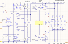
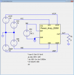
Here's a schematic I've been developing for a couple of months, now. I have not laid out the PCB yet, let alone built one.
[The schematic shown in post #92 is the most recent iteration so far.]
The design goal is a 200W amp with distortion below 0.001% up to 20 kHz. VCCP/VEEP looks like they're going to be +/- 63V unregulated. VCC/VEE will be +/- 70V regulated.
Generated rails from the shunt and series-pass regulators will be
VCCP-5V
VEEP+5V
+15V
-15V
I've made an attempt at EF-triple stabilization, with a thread here: Removing MJE1503x in an Output Triple
but I don't think the final answer to that can be found in sims. I have not drawn the feedback yet, nor the final compensation. In IC op amps, a cap from the top of R8 to GND is sufficient, but a T-miller arrangement here will further linearize the output stage.
OL Gain is very high, and the pole from the output stage will between 10 and 20 MHz.
Output transistor biasing will be adapted from William Chater's bias control circuit from 1988. That's what's in the yellow box. I've detailed my adaptation here:
William Chater's "Bias control for power amplifiers," Revisited
Added, 10 Mar 2020:
My plan is to finish this design, documenting my progress and performance on diyaudio. When the design is complete, and the PCBs are laid out, I will make PCBs available. Gerber files, too. Then I will try to stick around to give advice on building and mods.
I still have some expectation that simulated performance, up to 20 kHz can be as low as 0.001%. We will see if my PCB layout skills can get a real circuit to approach that performance.
At this point in my life, I have 35 years experience as a designer of audio circuits, including 12 years where I designed discrete transistor power amplifiers for car audio. After that, I designed class-B and class-D audio amplifier ICs for 10 years. Now, I am a research engineer designing analog to digital converters for 200 GS/s SERDES in silicon processes that are not yet released for production.
I'm hope this design ends up being as good as the best of what's out there, both commercially and DIY.
Outline of the thread, so far:
-----
keywords: [special=power amplifier]%[/special], [special=design ]%[/special], [special=folded cascode]%[/special], [special=triple EF]%[/special], [special=LTspice]%[/special], [special=low THD]%[/special], [special=low noise]%[/special], [special=self bias]%[/special]
.

Here's a schematic I've been developing for a couple of months, now. I have not laid out the PCB yet, let alone built one.
[The schematic shown in post #92 is the most recent iteration so far.]
The design goal is a 200W amp with distortion below 0.001% up to 20 kHz. VCCP/VEEP looks like they're going to be +/- 63V unregulated. VCC/VEE will be +/- 70V regulated.
Generated rails from the shunt and series-pass regulators will be
VCCP-5V
VEEP+5V
+15V
-15V
I've made an attempt at EF-triple stabilization, with a thread here: Removing MJE1503x in an Output Triple
but I don't think the final answer to that can be found in sims. I have not drawn the feedback yet, nor the final compensation. In IC op amps, a cap from the top of R8 to GND is sufficient, but a T-miller arrangement here will further linearize the output stage.
OL Gain is very high, and the pole from the output stage will between 10 and 20 MHz.
Output transistor biasing will be adapted from William Chater's bias control circuit from 1988. That's what's in the yellow box. I've detailed my adaptation here:
William Chater's "Bias control for power amplifiers," Revisited
Added, 10 Mar 2020:
My plan is to finish this design, documenting my progress and performance on diyaudio. When the design is complete, and the PCBs are laid out, I will make PCBs available. Gerber files, too. Then I will try to stick around to give advice on building and mods.
I still have some expectation that simulated performance, up to 20 kHz can be as low as 0.001%. We will see if my PCB layout skills can get a real circuit to approach that performance.
At this point in my life, I have 35 years experience as a designer of audio circuits, including 12 years where I designed discrete transistor power amplifiers for car audio. After that, I designed class-B and class-D audio amplifier ICs for 10 years. Now, I am a research engineer designing analog to digital converters for 200 GS/s SERDES in silicon processes that are not yet released for production.
I'm hope this design ends up being as good as the best of what's out there, both commercially and DIY.
Outline of the thread, so far:
- Addition of cascode below Q5. Discussion of TL431 and replacing with quieter infra-red LEDs--posts #8 - #15
- First documentation of performance--posts #15 - #28
- Simulated amplifier with clipping. Quasi-sat of KSA1220 driver caused instability exiting clipping. Replaced drivers with 4 each of KSC3503 and KSA1381. This let me increase UGBW to 5 Mhz from 3 Mhz, and increased SR to 94 V/us from 58 V/us. Posts #39 - #45.
- Documentation of simulated performance, post revision, Posts #46 - #50.
- Discussion with BesPav about my design decisions, Posts #62 - #65.
- Addition of SOA limiting, single-slope, dual slope, and eliminating distortion caused by SOA circuit, posts #66 - #78.
- Schematic of SOA limit and bias servo offloaded to daughter PCB, post #80.
- Replaced LM334 with "ring of two" current source, post #85.
- Find sources of distortion and optimize. TPIIC considered. Posts #92 - ...
-----
keywords: [special=power amplifier]%[/special], [special=design ]%[/special], [special=folded cascode]%[/special], [special=triple EF]%[/special], [special=LTspice]%[/special], [special=low THD]%[/special], [special=low noise]%[/special], [special=self bias]%[/special]
.
Last edited:
An imperious doodling indeed
You can use a figure 32 in the AD797 datasheet to simplify things.
Or just see attached pic.

I just noticed a pretty glaring mistake in that AD797 figure. gm should not be shown in the transimpedance amplifier.
Transconductance Amp is correct. Iout/Vin = gm. Units are 1/ohms
Transresistance Amp should be Vout/In = 1/(jwC), not gm/(jwC), Units are ohms.
The gain of the two stages multiplies together to give you gm/(jwC). Units are Volts/Volt (well, technically ohms/ohm).
Transconductance Amp is correct. Iout/Vin = gm. Units are 1/ohms
Transresistance Amp should be Vout/In = 1/(jwC), not gm/(jwC), Units are ohms.
The gain of the two stages multiplies together to give you gm/(jwC). Units are Volts/Volt (well, technically ohms/ohm).
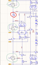
Earlier in this design development, I tried a cascode in series with Q5, with its base tied to ground. It actually hurt input offset to do that, which I found odd. Otherwise, it made no difference. In the final PCB, I'll will leave a hole for that cascode. If nothing else it will cut the power dissipation of Q5 in half, balancing its temperature with Q8.
I also tried bootstrapping the collectors of Q12 and Q13 to the Q19 and Q20 emitters. when I first put in the diamond buffer, and that did some very damaging things to the AC stability above 1 MHz. I'll be leaving those collectors tied to the rails.
I also tried bootstrapping the collectors of Q12 and Q13 to the Q19 and Q20 emitters. when I first put in the diamond buffer, and that did some very damaging things to the AC stability above 1 MHz. I'll be leaving those collectors tied to the rails.
@RussellKinder Could you shortly explain why you have choosen TL431 over the LED biasing? IMHO LED is very elegant lownoise tec.
Thx in advance.
If I remember correctly it (here somewhere) was discussed if the fc-100 could perform better with a dc servo but afaik Mihai said that DC offset is already very low and an DC Servo would contribute much. Since you compared your amp with this one - I want to ask how is the situation for your amp? (You already wrote that you have thought about improving it)
Your RK-Auto200W is a beast of engineering. Unfortunately my knowledge is not deep enough to understand thoroughly - but I already can sense the engineering effort went into the circuit...
After a long pause this raises urge to go back into this hobby
Btw nice hidding of the second beast in it
Hi,
Good question about the TL431 vs LED. TL431 is very low impedance and temperature stable, but noisy. For biasing cascode bases, the noise doesn't really matter. Also for biasing the 1st follower in the triple EF output, the noise is pretty irrelevant. It is eaten by the output impedance of the follower, and you are post gain at that point.
I'm usually not too concerned about tail current noise, because I mirror the current later on. That should cancel the tail current noise, mostly. I might consider something like Walt Jung's GLED-431 for the tail current. I don't really like glowing LEDs on my amp circuit boards, but I suppose I could paint them black
Super interesting! Thx for sharing.
You have sent me down quite a rabbit hole. Christer's posts on LED and noise of other references was very interesting. Ultimately, I came to two other links that I think are useful. One is a link to Walt Jung's page, where he has lots of useful pdfs, several on noise of references. The other is dicks_website.eu, where he systematically measures noise of several types of references, similar to Christer, but more rigorous, in my opinion.
Directory listing
Noise in voltage references
The bottom line here is that I have not really given much thought to the bias leg on the left side of my schematic. My first simulations were simply with 2.5V DC sources in place of the TL431s. Now that you have caused me to think harder about it, and do some research, I'm likely to change my biasing leg. I think I will replace the 33K resistor with an LM334, and the TL431s with stacks of two or three IR LEDs. I probably need to put a resistor or zener in series with the LM334, to absorb some voltage and power.
I could just as easily replace the two TL431 biasing the first EF in the output stage. Probably the next version of the circuit I post will have these changes made. I just need models for the LM334 and the IR LED.
Attachments
I have found some IR Parts Libs on the OSRAM Website. not the lite on HDSL..
Opto Semiconductors | OSRAM
I will have a thorough look at your links later - Im in a hurry now
Opto Semiconductors | OSRAM
I will have a thorough look at your links later - Im in a hurry now
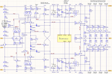
Watrix caused me to rethink my bias stacks, reminding me that TL431 shunt regulators are pretty noisy. Looking through Christer's thread on LED noise, Walt Jung's many articles, and Dick Kleijer's website (links in post #12), I decided to replace each TL431 with a pair of infrared diodes. A pair makes almost exactly 2.5V, and the noise will be about 40 times less. Not much of that noise would have come through into the differential signal path, but this revision probably gained a couple of dB SNR, overall. An LM334 sets the current in the bias leg, instead of a resistor. PSRR should be similar to a TL431 biased by a resistor.
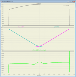
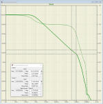
Attached is the revised schematic. A plot showing DC gain, output transistor current, and a wingspread diagram of the output stage is also attached.
Gain is about 100,000.
Total transistor bias current is 330mA, or 82.5mA/device.
Wingspread shows reasonably well-behaved transition across zero volts.
I've also added a simple 68 pF compensation cap and further tweaked the stability of the output stage. A plot of the open loop AC gain vs frequency is also attached.
Attachments
Last edited:
Also, so there's no mystery, here's my testbench in LTspice plus the schematic netlist for the amplifier.
I generate a netlist in Altium, put it in a subcircuit and link it with an LTspice symbol. The device models are all in the subcircuit.
The sharp eyed will notice that I'm nulling the open-loop offset by adjusting R7. This lets me null the DC offset without hurting the balance of input diff-pair. That has me thinking about an alternate method for wiring a DC offset nulling servo. I will have to investigate whether the majority of the DC offset comes from input pair mismatch or mismatch in Q6, Q7, and between Q12 & Q13.
In this sim, the offset comes from Q12-Q13 base current mismatch, and base currents of Q30, Q9, and Q7.
Attachments
Next step is closing the loop and a more sophisticated compensation network.
After I close the loop, I will develop the compensation in three steps, tracking distortion at each step.
After I close the loop, I will develop the compensation in three steps, tracking distortion at each step.
1) C to gnd from the output of the folded cascode. Folded cascode op amps with external feedback are often compensated this way.
2) Miller Input Compensation (MIC) to the amplifier's inverting input from the output of the folded cascode. The local loop may need some compensation.
3) Transitional Miller Input Compensation (TMIC) with a split C to the inverting input, and a resistor to the output from between the caps.
2) Miller Input Compensation (MIC) to the amplifier's inverting input from the output of the folded cascode. The local loop may need some compensation.
3) Transitional Miller Input Compensation (TMIC) with a split C to the inverting input, and a resistor to the output from between the caps.
Nice . I like the LM334 + IR LED solution. And it is astonishing fact that Dick Kleijer stacked up to 7 LED without seeing considerable noise.
I have just digged through the LM334 Datasheet. LM134 and LM234 seem to have slightly more accuracy but judging by your comment it might not really improve the performance. Hower fig. 30 in the TI LM334 Datasheet https://www.ti.com/product/LM134 shows some way to improve the output impedance by cascoding a fet. This would add some noise again but increases the output impedance. I don't know if the output impedance of the LM334 in this circuit is high enough. otherwise it could be improved by adding a pfet inbetween LM334 output (Source). D to D11 and gain behind R1.
. I like the LM334 + IR LED solution. And it is astonishing fact that Dick Kleijer stacked up to 7 LED without seeing considerable noise. I have just digged through the LM334 Datasheet. LM134 and LM234 seem to have slightly more accuracy but judging by your comment it might not really improve the performance. Hower fig. 30 in the TI LM334 Datasheet https://www.ti.com/product/LM134 shows some way to improve the output impedance by cascoding a fet. This would add some noise again but increases the output impedance. I don't know if the output impedance of the LM334 in this circuit is high enough. otherwise it could be improved by adding a pfet inbetween LM334 output (Source). D to D11 and gain behind R1.
Last edited:
Those are good ideas, but I suspect the circuit is good enough as is.
LM334 accuracy is unimportant. The amplifier will function the same even with a few 100 mV error from the nominal 2.5V of each LED pair, and the LEDs have very low dependency on the exact amount of current flowing. There is likely much more error in Vf variation among the LEDs.
Cascoding may have an important benefit: if I can find a cascode device with a large enough breakdown voltage, I can replace the resistor that I have protecting the LM334 from overvoltage. The LM334 is rated 40V, but the gap between the diode pairs is about 65V. I will look into it.
I wonder if there are any depletion FETs rated > 80V.
Looking through the LM334 datasheet, I see there are schematics for high current bandgap circuits, which would have much lower noise than TL431, 78xx, and similar circuits.
One more comment. The current from the LM334 is proportional to Kelvin. That may serve to offset the negative tempco of the LEDs slightly.
Last edited:
- Home
- Amplifiers
- Solid State
- RK-Auto200W Amplifer