I was also not very sucessfull with finding a suitable FET. ...massive series stacked diodes at gate x)
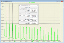
However please find attached your THD Data visualized. For Ploting I have used the free Matlab alternative Octave. Log is needed as csv.
Just a fast Plot script nothing fancy.
eps generated by the script have better quality. I do not use png a lot so sorry for the mediocre quality.
Need to refresh my ltspice skills then I will make thd analysis for Fc-100 and we could compare it. I have the spice data somewhere on my nas.
IMD Figures would also be interessting.
Attachments
Last edited:
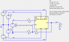
Attached is the revised schematic. A plot showing DC gain, output transistor current, and a wingspread diagram of the output stage is also attached.
Gain is about 100,000.
Total transistor bias current is 330mA, or 82.5mA/device.
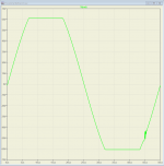
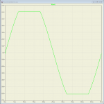
Wingspread shows reasonably well-behaved transition across zero volts.
I've also added a simple 68 pF compensation cap and further tweaked the stability of the output stage. A plot of the open loop AC gain vs frequency is also attached.
Nice OLG
OLG of FC-100
94db ~ 51000
RMI-FC100, a single stage audio power amplifier
OLG of FC-100 MKII (discontinued)
86db? but very flat
RMI-FC100 MKII, single ended folded cascode VAS
Last edited:
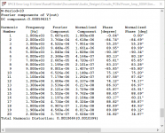
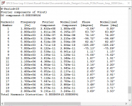
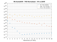
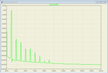
I have cranked up ltspcie again and used the original ltspice dataset of Mihai. His THD calculation have been a bit different compared to yours. So I changed it to 1kHz Plot of 20 Harmonics. Input amplitude is still 200mV as set by Mihai.
In comparison your Amp is looking really good. See yourself.
p.s. fc-100.zip is the LTspice Set. Comparison-fc-100.zip contains the pltoscript this time a bit more convinient with Harmonics # instead of pure freq.
btw...the THD is calculated by the script not necessary to copy past the result from Ltspce log.
Attachments
Last edited:
Nice OLG
Thanks. I see a way to get the DC OL gain higher, but compensation would increase with the gain, so gain-bandwidth would not go up. I have about 5V of headroom to play with at the top and bottom of the folded cascode. I can increase the emitter resistors R5, R6, R7, R9 (keeping current the same) in the top current source and the bottom current mirrors, and increase the gain. However, as Vce of the cascodes Q8 and Q9 gets low, their Cob can get an order of magnitude higher. If I keep the minimum Vce over 5V, Cob stays low.
GBW is set by the frequency response of the output stage. Even at 1 kHz, my distortion correction is limited by the GBW, and not the OL gain. I feel like I have squeezed all the bandwidth I can out of the triple-EF, while maintaining good stability. Maybe someone smarter than me could do better on OPS frequency response, but the smart guys seem to be saying that chasing OPS frequency response is not a good idea.
I believe that with transitional Miller input compensation, I can raise the 1st pole and reduce THD in the 1 kHz to 20 Khz range.
Step 1: Simple C to GND compensation
I have run several simulations on the closed loop. I initially closed the loop with a gain of 40, but I actually compensated it for a gain of 26dB or 20. I have changed the feedback for a gain of 20. That decreases the distortion from what I reported initially. Seems like all preamps are capable of 2V RMS output, and most are capable of over 10V RMS.
I have completed Step 1: C from the output of the folded cascode to GND. The C value is 68 pF, as shown in the schematic. BTW, that yields a calculated slew rate of 4mA/68pF = 58 V/us. A 60V amplitude, 20 kHz sine wave has SR=7.5 V/us.
Attached is
After I close the loop, I will develop the compensation in three steps, tracking distortion at each step.
1) C to gnd from the output of the folded cascode. Folded cascode op amps with external feedback are often compensated this way.
2) Miller Input Compensation (MIC) to the amplifier's inverting input from the output of the folded cascode. The local loop may need some compensation.
3) Transitional Miller Input Compensation (TMIC) with a split C to the inverting input, and a resistor to the output from between the caps.
I have run several simulations on the closed loop. I initially closed the loop with a gain of 40, but I actually compensated it for a gain of 26dB or 20. I have changed the feedback for a gain of 20. That decreases the distortion from what I reported initially. Seems like all preamps are capable of 2V RMS output, and most are capable of over 10V RMS.
I have completed Step 1: C from the output of the folded cascode to GND. The C value is 68 pF, as shown in the schematic. BTW, that yields a calculated slew rate of 4mA/68pF = 58 V/us. A 60V amplitude, 20 kHz sine wave has SR=7.5 V/us.
Attached is
1) Picture of the closed loop test bench,
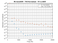
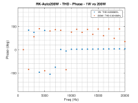
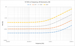
2) a plot of THD vs Freq for 1, 10, 100, and 200W, and
3) FFT at 1 kHz, 1W
4) FFT at 1 kHz, 100W
5) The .asc file of the testbench.
6) The netlist of the amplifier, in a .txt file.
The THD data shows that decreasing open loop gain above 600 Hz results in THD rising at 6dB/octave. The highest THD is 0.00633% at 200W, 20 kHz. I will see if Miller Input Compensation (MIC) or Transitional MIC will allow me to increase the loop gain at 20 kHz enough to get this number below 0.001%. That is the original design goal I stated in the first post of this thread.2) a plot of THD vs Freq for 1, 10, 100, and 200W, and
3) FFT at 1 kHz, 1W
4) FFT at 1 kHz, 100W
5) The .asc file of the testbench.
6) The netlist of the amplifier, in a .txt file.
Attachments
There is not going to be a step 2 or step 3 of the compensation. The other methods can get the same results as output compensation, but they cannot seem to do better. I iterated at length on Miller input compensation networks, but the best effort was identical to a simple 62 pF to GND from the FC output. That means there's no possibility of doing transitional Miller compensation, either.
Doug Self, on page 228 of his 6th edition amplifier design book, says (paraphrase) that he doesn't know much about designing folded cascode amps, but he does have one thing right. There is no Miller compensation, not even Miller Input Compensation.
I did tweak on the FC output compensation. I put 50 ohms in series with the 62 pF Ccomp, and I put 4.7 pF in parallel with the 12.1K feedback resistor. Ultimately, the THD results I've already shown are about as good as it's going to get. And frankly, that's not bad. Someone let me know if they have an amplifier that simulates or tests better than this one has, so far.
I did discover that Altium was not including C6, the 10uF cap between Q19 and Q20. I fixed that, and it helped THD by a tiny bit at 20 kHz.
It's time to put in protection circuits, output coil, bypass caps, and layout the PCB.
Someone let me know if they have an amplifier that simulates or tests better than this one has, so far.
Heh...
First one - rewire it's external circuitry to overall amp be inverting.
Keep in mind very simple idea, noninverting amp's inputs are always at some common mode voltage. No way to exclude this. Nothing critical, but any amp have common mode error and such an error are nonlinear with common mode itself. But, stop, one says, common mode is our signal, aren't it?
Yes. You just add signal-related error just by choosing noninverting connection.
Inverting amp track difference between groung and input-(output/gain) and in real world with parasitics are better just by topology.
I have run several simulations on the closed loop. I initially closed the loop with a gain of 40, but I actually compensated it for a gain of 26dB or 20. I have changed the feedback for a gain of 20. That decreases the distortion from what I reported initially. Seems like all preamps are capable of 2V RMS output, and most are capable of over 10V RMS.
I have completed Step 1: C from the output of the folded cascode to GND. The C value is 68 pF, as shown in the schematic. BTW, that yields a calculated slew rate of 4mA/68pF = 58 V/us. A 60V amplitude, 20 kHz sine wave has SR=7.5 V/us.
Attached is
1) Picture of the closed loop test bench,The THD data shows that decreasing open loop gain above 600 Hz results in THD rising at 6dB/octave. The highest THD is 0.00633% at 200W, 20 kHz. I will see if Miller Input Compensation (MIC) or Transitional MIC will allow me to increase the loop gain at 20 kHz enough to get this number below 0.001%. That is the original design goal I stated in the first post of this thread.
2) a plot of THD vs Freq for 1, 10, 100, and 200W, and
3) FFT at 1 kHz, 1W
4) FFT at 1 kHz, 100W
5) The .asc file of the testbench.
6) The netlist of the amplifier, in a .txt file.
")
You can look at this amp, I prefer CFA and a bit different compensation.
https://www.diyaudio.com/forums/solid-state/253039-unique-cfa-120-230w-amp-26.html#post4668890
The left channel will be non-inverting. The right channel inverting.
What about stereo image?
The CMRR of this amp is so high and extended in frequency that your assertion is ridiculous.
Yes, CMRR will be enough.
The common mode error of an amp with a gain of 20 and high impedance tail current is negligible.
DMMT5551 and 2n5551 datasheets doesn't contain static characteristic graph, but you can see for interest something like BC550/560 or 2n3904/6.
The main interest here will be Early effect related dependance of the collector current vs collector-base voltage.
They share current with next stage KSAs, but one of them under full rail spread, while second under only half, sharing voltage rails with lower KSC.
Please, let me know your opinion - what's the main source of distortion in audio amplifiers?
You can look at this amp, I prefer CFA and a bit different compensation.
https://www.diyaudio.com/forums/solid-state/253039-unique-cfa-120-230w-amp-26.html#post4668890
That THD is certainly in the same ballpark. Nice CFA amp.
What about stereo image?
I simply reverse the labels on the right channel speaker terminals to fix the polarity. Doing this has two benefits: 1) the amp automatically bridges to mono by using the L+ and R- terminals. 2) the two channels draw their currents from the opposite supply rails, reducing voltage sag on the rails and cutting in half the peak current in the rectifiers.
I suppose if I did a PSU design with two sets of rectifiers and two sets rail caps, this would not matter.
DMMT5551 and 2n5551 datasheets doesn't contain static characteristic graph, but you can see for interest something like BC550/560 or 2n3904/6.
The main interest here will be Early effect related dependance of the collector current vs collector-base voltage.
The emitter degeneration of the KSC3503 current source multiplies the Early voltage of the KSC3503 by beta*(RE/(RE+Rpi)). If I use E grade KSC3503, min beta = 100. Looking at the char. curves, VA is already very high, but let's say it's 500. Rpi is 650, so the effective VA becomes 21,000, and Ro of the tail current source is 500,000. A couple of volts common-mode will change the 4 mA tail current by less than 4uA.
The Early voltage of the MMBT5551 cascodes is also multiplied by beta * Ro of the SSM2212 device. The SSM2212 datasheet shows shows Ro at 2 mA is 50 Kohms. Whatever the Early voltage of the MMBT5551 is, it's going to be multiplied by at least 3 million, due to the cascoding. Common-mode swing will have virtually zero effect on the small-signal parameters of the MMBT5551 transistors.
They share current with next stage KSAs, but one of them under full rail spread, while second under only half, sharing voltage rails with lower KSC.
Please, let me know your opinion - what's the main source of distortion in audio amplifiers?
The KSA1381 cascode devices are no less linear than a CE VAS stage with similar output impedance.
The main source of distortion in BJT amplifiers is dependency of small-signal parameters on collector current. The better the circuit is able to hold Ic constant, the more linear it will be. The keys to this are signal independent biasing, and high impedance at the VAS output. KSA1381 device Q8 has 2.4mA bias current. With 113V voltage swing, it's current swing is 26uA.
An easy experiment is to cascode the tail current, and see the effect this has on THD.
Another good designer I knew back in the mid-1990s, Robert Zeff, also promoted the use of amplifiers in their inverted configuration. And for the same reason. I said a good tail current source nulls the effect. He said, if you invert, there's no effect to null. So, in principle, you have a good point about the inversion.
Another good designer I knew back in the mid-1990s, Robert Zeff, also promoted the use of amplifiers in their inverted configuration. And for the same reason. I said a good tail current source nulls the effect. He said, if you invert, there's no effect to null. So, in principle, you have a good point about the inversion.
I ran that experiment, cascoding the tail current. With a 20kHz 200W output, these are the distortions, before & after:
No cascode: 0.00479% THD
With cascode: 0.00482% THD
So, the THD went up a little. I attribute this to the slight loss of tail current due to beta/(beta+1) of the cascode device. My conclusion is that cascoding the tail current does not change the THD at all, all else held equal.
Cascoding might help if the supplies are trashy, but I plan on regulating these, either from a 2nd transformer or from a clean switching supply.
Last edited:
Clips of clipping
Hey, kids, guess what time it is? It's time to clip the amplifier.
I set a signal to clip at just over 10% THD. It's all graceful except for the squiggle at 45us. I investigated and found this problem is due to quasi-saturation of Q20, the KSA1220. I gave Q20 2 extra volts on its collector, and the problem disappeared. I'm using keantoken's models. Perhaps he will wander by and comment on it.
This is either an anomaly of the model, or I need to find an alternate device to the KSA1220. Comments welcome.
Attachments
- Home
- Amplifiers
- Solid State
- RK-Auto200W Amplifer