Well all done.
Just need to find some schematics online with voltages current readings give me something to go by. Not plugging anything in until then.
Then fan switches go in.
Noticed the BF470 and 469s been changed at some stage apart from one so something went wrong.
Here’s a module have a pair mainly Texas instrument components. What you make of it? Looks to be good bit of kit.
Thanks for input all really appreciated.
Attachments
Mighty purdy .. 
I think I know what you mean about medication adding extra space between neurons -- though it seems I've been a little luckier than you, so far anyway .. Sorry to read of your prognosis; glad that you have this most lovely diversion.
The 2SD424 / 2SB554 outputs ARE BJTs, by the way -- so I was only half right! .. and the schematic will be totally different.
Congrats, Cheers
I think I know what you mean about medication adding extra space between neurons -- though it seems I've been a little luckier than you, so far anyway .. Sorry to read of your prognosis; glad that you have this most lovely diversion.
The 2SD424 / 2SB554 outputs ARE BJTs, by the way -- so I was only half right!
.. and the schematic will be totally different.Congrats, Cheers
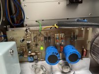
Well just noticed few things not adding up. The transistors that where replaced on left module I think I know why. The replaced caps are rated 63vdc now unless its a mistake on schematic they should be 70vdc I've also put in 63vdc on jot havinga schematic so I'mgonna put some 100vdc in there. Em now I'm getting over 63vdc readings on the diode bridge plus some of the resistors are different values. R13 is a 2 watt metal film rated at 12k it is only 6.8k now that's running between the transistors thats nearly half so voltages gonna be higher than should be and the readings are jumping all over the place there. So thats gonna need changing funny it's not marked as 2 watt metal film? Plus some of the other resistors are of different value but 90% adds up in relation to the schematic. So RS jobby today I might even up the capacitance to 6800uf.
Odd someone has had a play. More time waiting on parts. The 100uf caps I'm only getting mV readings on +ve side would that be correct? Mind you no load has been applied yet glad it ain't. Any thoughts?
Odd someone has had a play. More time waiting on parts. The 100uf caps I'm only getting mV readings on +ve side would that be correct? Mind you no load has been applied yet glad it ain't. Any thoughts?
More info R11 & R12 are listed as 100r both installed are 200r? R14 marked 100r again there's a 0r in there running to 0v but even so why put 100r on schematic but put 0r in. I know it's running to the 0v track so why not just put the leg of the BF469 straight to 0v? If not needed.
Checking Buzz and BJts specs same apart from amps bjts 7 amps buzz 8 amps? So 1000 mA difference that's all I can think of is why there's a 0v there.
Anyhow I'll put correct values in plus after extensive searching managed to get some original 2sa872s, bf469 & bf470s so those on left module with painted lines on will also get changed out. See what happens. Could be waste of money but all bout trial and error be interesting to see if output mV drops. Decided to stick with 4700uf caps but now 100v. Do have some but rated at 450v bit pointless putting them in never gonna get near 100v let alone 450v.
C3 is fine those are actually new the 100ufs. Whats also interesting is C7 is a poly 400v now why would that be in there at that rating? Does that mean you could get a spike of 400v on the output side?
Anyhow still ongoing ha ha. But get it right then all external equipment is at least safe from any damage. Definitely don't wanna be blowing decent speakers for sure.
All good fun and enjoyable. So easy to work on but looking at the module it looks so basic but more complicated than first anticipated even heatsinks depending on heat dissipation need to be a certain spec watt wise initially I'd of thought just stick bit ali in there whack on transistor job done. Even there calculus comes into play.
The mV DC readings are normal for both 100uF caps.
The 0R replacing R14 (schematic shows 100R), which feeds the Emitters of the BF469's is probably because both of those transistors would be off otherwise! The value of the installed R5 is what I want to know; it sets all the operating currents all the way through, except the outputs. At the 10k the schematic shows, a little napkin arithmetic shows only 110uA for TR's2 & 3 to share. 55uA only produces a 260mV drop across R7 and R8, which won't put the BF469s in any sort of good-conducting mood at all -- even if you leave R14 at 0R. (Also, note that it connects to the negative rail, not ground or 0V.)
If you set all the resistor values per the schematic, it simply won't pass a signal.
I recommend replacing R5 with a much smaller value, say between 3k9 and 560R, depending on how much heat you're willing to tolerate in the BF469/470's.
Replacing the transistors that are in pairs (BF469, BF470) may not be a good idea: The originals are surely better matched than arbitrary replacements would be, and matching is what makes that part of the circuit work properly.
C7 being 400V is all about its ability to handle sustained high ripple currents without overheating. If it fails open, the channel will probably break into ultrasonic oscillation (not good).
The 0R replacing R14 (schematic shows 100R), which feeds the Emitters of the BF469's is probably because both of those transistors would be off otherwise! The value of the installed R5 is what I want to know; it sets all the operating currents all the way through, except the outputs. At the 10k the schematic shows, a little napkin arithmetic shows only 110uA for TR's2 & 3 to share. 55uA only produces a 260mV drop across R7 and R8, which won't put the BF469s in any sort of good-conducting mood at all -- even if you leave R14 at 0R. (Also, note that it connects to the negative rail, not ground or 0V.)
If you set all the resistor values per the schematic, it simply won't pass a signal.
I recommend replacing R5 with a much smaller value, say between 3k9 and 560R, depending on how much heat you're willing to tolerate in the BF469/470's.
Replacing the transistors that are in pairs (BF469, BF470) may not be a good idea: The originals are surely better matched than arbitrary replacements would be, and matching is what makes that part of the circuit work properly.
C7 being 400V is all about its ability to handle sustained high ripple currents without overheating. If it fails open, the channel will probably break into ultrasonic oscillation (not good
).
Last edited:
So I can measure mA across R5? Still not sure where I'm gonna get the mA readings from apart from pulling fuses and measuring across there why im asking.
Don't understand why schematic has the different values then! Must be a reason? So reducing from 200r to 100r not gonna let signal through?
0r again don't get that at all why put it there if not needed?
Thats good re 100uf caps. Not used to seeing such low values.
Interesting re poly I'm used to the psu caps covering ripple did not realise the transistors need protecting. Gets more complicated as things move on.
The 100r resistors out of spec so obviously been running hot.
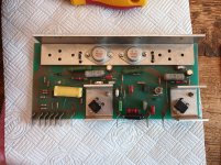
PR1 well measured both interesting right module set at 336r left leg and 0.3r right leg looking from front.
The other module PR1 set at 46.8r left leg and 0.1r right leg explains voltage differences.
Ordered complete new set of the BFs and 2SAs. But not gonna change all of them it's just the originals which I've sourced are not copies and are scarce so makes sense to have a spare set. The only ones to be changed are the ones on left module the black ones painted with lines on top they are not the original grey ones. Those obviously went at some stage. As did the psu caps evidence of splatter on modules. Ex DJ gear from 80,s so they have been run pretty hard I would have thought. The H&H speakers I got dust caps had blown out think speaks for itself. Another one I have all psu caps leaking everywhere and all fuses blown. Again run hard. But thats what they where designed for.
I'll give that a go re R5 going that low just into 500r mark from 10k seems huge drop! But heat not a problem as the fan will cover that.
So to sum up where do I get mA readings? leave all others resistors as they are except R5 and obviously re set PR1 and put in new 100r resistors I'll put 3 watt in, put fan modules in cement thermosistor to heatsinks wire all in, plus put some avro pins in for the main tranny wires so can attach top side easier access if need to lift board off.
Seems about it. But maybe that schematic was an upgrade from the original? All I can think of or misprints.
Don't understand why schematic has the different values then! Must be a reason? So reducing from 200r to 100r not gonna let signal through?
0r again don't get that at all why put it there if not needed?
Thats good re 100uf caps. Not used to seeing such low values.
Interesting re poly I'm used to the psu caps covering ripple did not realise the transistors need protecting. Gets more complicated as things move on.
The 100r resistors out of spec so obviously been running hot.
PR1 well measured both interesting right module set at 336r left leg and 0.3r right leg looking from front.
The other module PR1 set at 46.8r left leg and 0.1r right leg explains voltage differences.
Ordered complete new set of the BFs and 2SAs. But not gonna change all of them it's just the originals which I've sourced are not copies and are scarce so makes sense to have a spare set. The only ones to be changed are the ones on left module the black ones painted with lines on top they are not the original grey ones. Those obviously went at some stage. As did the psu caps evidence of splatter on modules. Ex DJ gear from 80,s so they have been run pretty hard I would have thought. The H&H speakers I got dust caps had blown out think speaks for itself. Another one I have all psu caps leaking everywhere and all fuses blown. Again run hard. But thats what they where designed for.
I'll give that a go re R5 going that low just into 500r mark from 10k seems huge drop! But heat not a problem as the fan will cover that.
So to sum up where do I get mA readings? leave all others resistors as they are except R5 and obviously re set PR1 and put in new 100r resistors I'll put 3 watt in, put fan modules in cement thermosistor to heatsinks wire all in, plus put some avro pins in for the main tranny wires so can attach top side easier access if need to lift board off.
Seems about it. But maybe that schematic was an upgrade from the original? All I can think of or misprints.
Measure DCR of R5 with the power off (since there have been others that disagreed with the schematic). Then, if TR1 and the LED are operating properly, the voltage across it will tell us the current. Maybe try 3k9 or 3k3 before diving straight to the 560R; the only reason for suggesting the range was to avoid having you get 'mail order blocked', where all work stops due to the lack of a particular-value 5 cent part.
I wouldn't increase the power rating of the 100R resistors (assuming we're both talking about R11 and R12) -- they're only dissipating a few mW, to up to a couple-10's of milliwatts in normal operation. By stretching, they're saving the semiconductors. Sort of a 'soft fuse'.
You need to find another schematic for the module with bipolar outputs and TIP33/34 drivers on their own heat sinks. Driving BJT's is a whole 'nother project from driving lateral MOSFETs. At the least, the bias pot values won't be comparable. Probably most of the resistor values after the input differential pair will be different, as well.
Before powering up after changing any resistors, make sure the bias pot is set to minimum -- that is, its lowest value, substantially holding off the outputs. Voltages to ground will not represent much at that moment. Until the outputs begin conducting, which closes the feedback loop, most of the VAS is high-impedance. Measurements will jump around, varying from EMI, leakage currents, and whatever else the probe-holder's other hand is touching.
This design is a little light for DJ use in the 1980's. I'd be a little surprised if that's what did it in. There were some pretty big amps coming out by then -- and cheap!
Cheers
Last edited:
Sorry, just thought of it: LED's are not as rugged as ordinary PN junctions. One of the earlier failures may have briefly exposed the LED to more reverse bias than the usual limit of a few volts. That invariably 'softens the knee', which would further reduce the already low current through R5.
If its a red LED, R5 should have about 1,1V across it. Does it?
If its a red LED, R5 should have about 1,1V across it. Does it?
And .. when it comes to discrepancies schematic <<>> equipment, there are at least two possibilities, both fairly common.
- a technician altered it during a previous repair
- the original draftsman made a boo-boo
I suggest R4 / R5 as kinda likely for the latter -- R4 is so low that any rail voltage higher than ~38V will exceed the forward current rating for LEDs of that vintage - 30mA. If it were 10k, the LED current would be in the 3mA range -- much more reasonable, and plenty to keep TR1 happy.
If R5 were 1k2, instead of 10k (that the schematic shows), the current available to the long-tail pair would be around 1mA -- much more reasonable than the 110uA it would be by the values in the schematic.
R14 replaced by jumper may very well have been a test. The 4 transistors of the VAS -- TR's4, 5, 6 and 7 -- may have all been biased off, maybe due to damage caused by other failures. At that point jumpering R14 would at least allow it to pass signal, though it wouldn't be the desired quality. The VAS can't operate properly without about 600mV of forward bias, Base to Emitter; then R14 can start insisting that TR6 and TR7 share the same current. Since 600mV across 4k7 (R7 and R8) requires a current of ~128uA, below that the VAS simply won't work.
Cheers
Okay cheers guys Lot if info to digest there. I'm not too concet6about the other module with the tips on so thats on back burner. Want to get this pair set up first before any work on other pair. Measure DCR of R5 module switched Off?
LED not measured yet.
R11 & R12 have both been swapped the 100r resistors are now 200r resistors not the 100r as listed on schematic. But sure someone said leave them in! I was gonna put 100r resistors back in there.
Get PR1 switching right down before switch on.
I have some 1k2 for r5 1/4 carbon film. Can do that.
All this gear is from 70,s except these modules think where first made in 1980! I have mixers a vortexion 50/70 fet plus other gear got it all as job lot. The vortexion is mint in beautiful condition only draw back its 100v line non switchable. Pain.
But don't wanna go of track so modules removed some parts coming today.
The PR1s especially the left module way low resistance compared to other.
Okay digestion on info going on. Ha ha not literally ��
That’s okay threw me a bit. R5 is 10k on +ve rail now I have some 3.9k which I could put in so that’s gonna increase voltage to the TR1. So that’s the objective? So what voltage should I expect? Or are we looking at Current?
I’ve had to put new PR1s in as they where jumping all over place out of circuit and resistive drop was inconsistent. So knackered.
R15 & R16 again odd in circuit are 220r but on schematic there 470r? But I assume you could put 100rs in there?
R13 I have changed out again hon schematic 12k in circuit 6.8k? I think 12k would be correct plus I noticed on removing them they have burnt the board underneath so obviously been getting hot and considering the TRs been replaced suggests too much heat there. Just an assumption but also noticed the same on the other module.
Put in new psu caps almost 5 amp ripple anti surge 100v so gives me piece of mind. Otherwise nothing else needs doing. Moved pins from beneath board to topside so can get direct measurements off mains transformer wires no good underneath. Not sure why whoever did it put them there plus easier if need to get module off.
So let me know then I can hook up. Turn trimmer think be fully anti clockwise before switching on and put some 1 amp quick blow fuses in initially. If they go at least know something wrong so circuit protected plus quick switch off.
Cheers Rick
Your 3rd question nailed it -- Current. If the circuit is working properly, the forward-biased LED approximately matches the temperature coefficient of TR1's Base-Emitter junction; it's called a CCS -- Constant Current Source.
There's another issue that affects the CCS -- how healthy is the LED? It should be cranking out a lot of light powered by the 1k2 to ground. And 35 mA is a lot for a 1970's LED. If it is not extremely bright, it is almost certainly failing. That'll reduce the resulting CCS current, too.
The design suggests something in the neighborhood of +/-38 to 46V rails; if they are higher, somebody probably thought increasing the output power was a simple matter of jacking up the rails.
A lot of the good folks on here are keen on -- and I don't remember what they call it -- a Light Bulb Tester for initial power-ups. If your IEC has spade terminals, there's no need to 'build one' -- just grab a retired standard socket and fit one male and one female spade terminal. Then put a 40, 60 or 100W incandescent bulb (depending on how brave you are) in the socket and hit the switch. If it flashes but goes dim, time to check some voltages; start at the rails. If it stays bright, or even mostly, you still have problems.
Regarding the bias trimpots .. although it is convention that the CCW position is minimum bias, better to comfirm with the ohmmeter. Depending on the design, maximum bias can kill drivers/outputs even with the Light Bulb Tester.
Regards
edit: Forgot to say, "Glad you changed out the PR1s/bias pots." Nothing releases the magic smoke like a flaky bias pot.
Last edited:
Cheers Rick
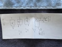
Yes I think the trimmers need to be fully CWW gives me 1k going across the right leg and CW gives 1k across left leg looking from wiper forwards plus right leg goes off to nothing as per schematic. Pic attached of original readings of one of the original trimmers. But the right leg has the highest resistance. But that would mean fully anti clockwise.
Now do I leave R5 as 10k? Or drop down to 3.9k? So is R5 fixed for quiescent current or PR1 adjusts that as well as bias which is obviously not fixed on this unit but seems the two are treated differently in the circuit unless I’m reading too much.
Yes I have a bulb limiter made up obviously working mainly on valve gear handy bit of kit although I’ve seen split wires leaking caps and burnt resistors on circuit and bulb still goes dim meaning nothing wrong with circuit em!!! Really just limiting power to unit. I’ve got a variac which I use to wind up the circuit over 6 to 10 hours. Gives everything time to warm up slowly talking valve circuits here not transistors circuits as all new to me low voltage high current other way round to what I’m used to.
But looks like you need to let this circuit run for hour check voltages etc adjust and run again and if needed adjust again. Seems to be more associated with the output readings!
Cheers Chris
Yeah, the bulb limiter doesn't give a complete diagnosis. But it does save some of the expensive parts from a life shortened by some of the easier-to-make errors.
Am still studying your pic. This is describing the PR1 bias trimpots on the MOSFET-based modules?
I wouldn't let an hour slip away waiting for voltages to settle. See what the rails are, then start confirming that other voltages are reasonable, either by proportion to the rails, or their own voltages independent of the rails.
I can't answer any specific questions about a reasonable value for R5 until we know the condition of the LED. There is a range of reasonably optimum current values for the input differential pair, and another for the output pair. And they are one-way interactive, going *front to back* -- the current from the input-pair-CCS affects the bias, but the bias changes don't affect input current. The important one - the one that keeps the magic smoke inside the transistors - is the output bias. Since the designer didn't provide one, I recommend interrupting (temporarily) either the Drain leg of each output device (connects to the rail), or the rails themselves, with a 0r10, 0r15, 0r22, or 0r33 resistor -- non-inductive if you can get 'em -- 1 watt is big enough. At that point we'll be ready to make well-informed decisions concerning bias.
There are designs that attempt to vary bias according to signal conditions. This is not one of them. Those units have 10 to 25 times the complexity of these.
Still waiting to hear what the voltage across R5 is, as well as the rail voltages. I still think it's too likely that the draftsman swapped the values of R4 and R5. 1k2 gives way too much current through the LED. An R5 of 10k provides way too little current for the differential pair, and subsequently the Bases of TR6 and TR7. The output offset will jump around quite a bit -- and mean almost nothing.
Sorry it's taken me a while to get this back to you.
Cheers
Last edited:
Okay got ya yes I think I’m looking to get the output on speaker terminals at or as near to +/- 0v DC. I also need to get resistance of emitter resistor then mV reading then do the math. Think quiescent current need adjusting to 50mV initially. So per transistors could we be looking at getting over 150mV then adjusting DC offset. But I’ll go with your points see what we get. Waiting on post at moment for parts bloody nightmare had none for 5 days now covid issues at the sorting office. All other postal services running fine. Should of got all me bits off RS always get it next day. Obviously not transistors obsolete. Def need new leds there the 10mm ones.
Green LED is 2.2 forward voltage and 25mA. Slightly higher than the reds.
Might bite bullet and get new ones off RS. But wanted new transistors in as pointless setting it all up only having to do it all again.
Sure those BFs should have small heat sinks on them as there burning the pcb where there obviously been getting incredibly hot.
Still just waiting game now. But it’s odd circuit looked at probably 50 schematics but have not found one that matches that layout at all.
- Home
- Amplifiers
- Solid State
- b k electronics mosfet 100 watt modules