Ssassen, you asked for a link to the GEM amplifier branchThanks petr_2009, can you point me towards the schematic of the Graham amplifier you refer to? I'd like to simulate it and compare it to my own design, as I'm always open to new ideas and there's a good chance I'll learn something in the process.
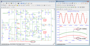
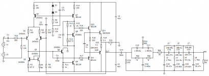
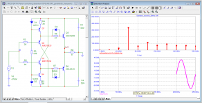
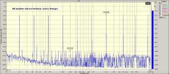
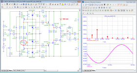
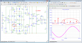
here is a simplified version of the amplifier
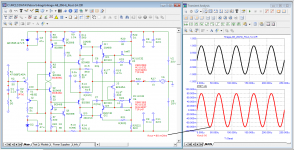
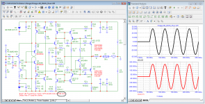
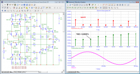
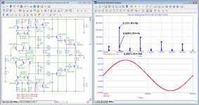
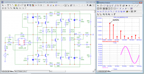
The GEM amplifier
The GEM amplifier
p.s.
I still don't understand why some of my tests of your amplifier were removed from your branch and I was banned. If my tests are incomprehensible to someone, this does not mean at all that they are not interesting to anyone and not instructive.
regards
Measuring the output impedance of an amplifier
In practice, three methods are used:
1. The simplest and most commonly used method is as follows.
Measure the voltage at the output at no load Vno_load (no load Rl) and at the load Vl. Then the output impedance is calculated using the formula: Rout = Rl*(Vno_load - Vl) / Vl
2. The second method is convenient for use in simulators.
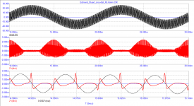
Short the amplifier input to ground. The output of the amplifier is supplied with alternating current of the frequency at which we want to measure the output impedance. If you apply a current of 1 Ampere, then the output voltage will be equal to the output impedance in ohms. A 1000 V voltage source and a 1 kΩ resistor can be used as a 1 A current generator. Delay line X7 used for clarity
3.The third method is often used in both hardware and simulators. As in the second method, the amplifier input is shorted to ground. At the output of the amplifier, between the load (Rl = 8 ohm) and ground, a voltage source is switched on with an amplitude of approximately ¾ of the supply voltage and the voltage at the output of the amplifier is measured. When measuring real amplifiers, use the second channel of the stereo amplifier. The output impedance is calculated using the formula: Rout = Rl * Vout / (Vin-Vout)
Of the three methods, in my opinion the most useful and informative is the third method. Observation of the voltage at the output of the amplifier together with the generator signal is done using a two-channel oscilloscope.
In practice, three methods are used:
1. The simplest and most commonly used method is as follows.
Measure the voltage at the output at no load Vno_load (no load Rl) and at the load Vl. Then the output impedance is calculated using the formula: Rout = Rl*(Vno_load - Vl) / Vl
2. The second method is convenient for use in simulators.
Short the amplifier input to ground. The output of the amplifier is supplied with alternating current of the frequency at which we want to measure the output impedance. If you apply a current of 1 Ampere, then the output voltage will be equal to the output impedance in ohms. A 1000 V voltage source and a 1 kΩ resistor can be used as a 1 A current generator. Delay line X7 used for clarity
3.The third method is often used in both hardware and simulators. As in the second method, the amplifier input is shorted to ground. At the output of the amplifier, between the load (Rl = 8 ohm) and ground, a voltage source is switched on with an amplitude of approximately ¾ of the supply voltage and the voltage at the output of the amplifier is measured. When measuring real amplifiers, use the second channel of the stereo amplifier. The output impedance is calculated using the formula: Rout = Rl * Vout / (Vin-Vout)
Of the three methods, in my opinion the most useful and informative is the third method. Observation of the voltage at the output of the amplifier together with the generator signal is done using a two-channel oscilloscope.
Attachments
Output stages of class AB are characterized by switching distortion. To reduce this type of distortion, there are technical solutions without cutting off the collector current of the output transistors, for example:
Patent US4595883
https://www.edn.com/the-class-i-low-distortion-audio-output-stage-part-3/
Let's check the parameters of one of these solutions
Class i and siblings
Patent US4595883
https://www.edn.com/the-class-i-low-distortion-audio-output-stage-part-3/
Let's check the parameters of one of these solutions
Class i and siblings
Attachments
-
 Class-i_crossover-distortion_RL-8.png30.8 KB · Views: 101
 -
 Class-i_crossover-distortion_RL-4.png28.4 KB · Views: 101
 -
 Class-i_IMD_19-20kHz.png30.8 KB · Views: 141
 -
 Class-i_20kHz-THD.png85.2 KB · Views: 171
 -
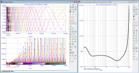
 Class-i_20kHz-spectr_(R1-100_1k_5k).png85.4 KB · Views: 485
 -
 Class-i_Bode.png34 KB · Views: 485
Last edited:
Let's make an output stage according to the idea:
New Lineup IDEA - Power Follower/Output stage
New Lineup IDEA - Power Follower/Output stage
Attachments
-
 OPS_RM2014-05_Rout.png86.7 KB · Views: 152
 -
 OPS_RM2014-05_cross-dist_(RL-4).png29.7 KB · Views: 126
 -
 OPS_RM2014-05_cross-dist.png31.8 KB · Views: 115
 -
 OPS_RM2014-05_IMD_19-20kHz.png28.1 KB · Views: 150
 -
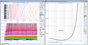
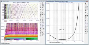
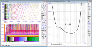
 OPS_RM2014-05_20kHz-THD_(R1).png89.6 KB · Views: 194
 -
 OPS_RM2014-05_20kHz-THD.png87.5 KB · Views: 184
 -
 OPS_RM2014-05_Bode.png26 KB · Views: 125
I agree with Hans. The charts you are sharing aren't done in a conventional way... at least not the convention that users of this forum are accustomed too. As a result, it's not always clear what you are trying to convey... especially when descriptions accompanying the charts are brief or nonexistence.
Also keep in mind, users of this forum have varied backgrounds. Many of us are not engineers and many are novices. This should be a place where people can learn and not feel like they'll be dissuaded from asking questions.
Also keep in mind, users of this forum have varied backgrounds. Many of us are not engineers and many are novices. This should be a place where people can learn and not feel like they'll be dissuaded from asking questions.
I hope there is no need to explain what a distortion spectrum is in the form of a Fourier expansion The same goes for intermodulation distortion. Under each chart there are captions explaining what they display.You deserve the price for producing images in a way that most if not all of us don’t understand.
Why not describing each picture like everybody else does by telling which line is showing what and why and then coming to some sort of conclusion.
Hans
As for the conclusions, then you can compare the parameters of the two amplifiers with each other
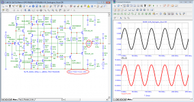
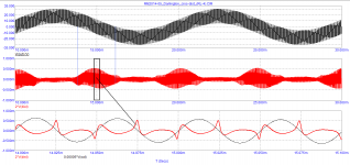
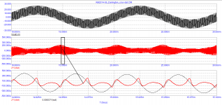
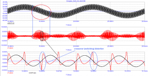
If I understood correctly, many people do not understand the results of tests on measuring switching distortions. I have repeatedly given the filter circuit with which the measurements were made, I am citing it again. I think you can use such a filter in any simulator. The only thing you need to know: start outputting measurement results after the end of the transient processes in the filter, not earlier than 10 ms. See also the description of the application of the virtual device for measuring switching distortion. As an example, we measured the output stage of the DartZeel-108 amplifier.
Attachments
O.K. thank you for responding.
I have read your PDF and understand you are dividing the areas of investigating in three parts, the positive halve, the zero crossing area and in the negative halve.
The idea to see the different behaviour in these three areas is quite nice and brings me to a number of questions.
1) In the PDF you presented, the distortion envelope for the Dartzeel looks as if modulated by 20Khz.
Why is this 20Khz envelope not filtered by your notch filter ?
It would be interesting to have some form of explanation why.
Using an FFT could reveal more detail.
2)In the zero crossing area you blame the distortion to switching distortion alone.
But what about IMD and THD ?
Again an FFT (for the three different areas) could give some answers.
3) It's nice to see what happens when using 100Hz + 20Khz, but it has hardly any impact on Audio reproduction since it's all above 20Khz and completely supersonic.
So why not somewhere in the low Khz range, where our auditory system is most sensitive ?
Hans
Hans, the use of the FFT shows the spectrum of distortion products, but does not provide a visual representation of the causes of these distortions.
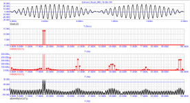
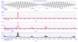
The more you use such a filter in your tests, the more you will become convinced of its usefulness. For example, test the output stage using a single frequency of 20 kHz. You can see how the amplifier works asymmetrically at zero crossing.
Here are two tests of the same amplifier with the same signal.
In the FFT spectrum, we see the frequency of harmonics, but the reason for their occurrence is not clear.
The filter test complements the FFT test perfectly.
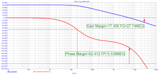
When designing an amplifier, I do not limit myself to checking the Bode diagram, loop gain and THD, but do many other tests.
The more you use such a filter in your tests, the more you will become convinced of its usefulness. For example, test the output stage using a single frequency of 20 kHz. You can see how the amplifier works asymmetrically at zero crossing.
Here are two tests of the same amplifier with the same signal.
In the FFT spectrum, we see the frequency of harmonics, but the reason for their occurrence is not clear.
The filter test complements the FFT test perfectly.
When designing an amplifier, I do not limit myself to checking the Bode diagram, loop gain and THD, but do many other tests.
Attachments
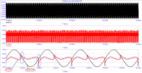
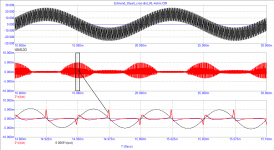
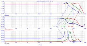
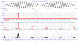
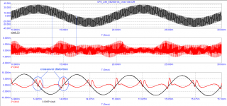
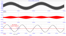
Let's continue our study of amplifiers using a filter. Here is another example of an output stage positioned as an OPS with distortion compensation. Let's see how it copes with switching distortion, as well as the spectrum of signal distortions with a frequency of 20 kHz.
as you can see, the output stage does not handle switching distortion very well
as you can see, the output stage does not handle switching distortion very well
Attachments
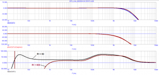
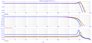
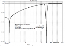
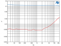
If you look at the dependence of distortion on frequency, you can see a rapid increase in distortion starting at a frequency of 2 kHz. With a signal source resistance equal to 50 Ohm to a frequency of 20 kHz, distortion reaches the level of 0.025%. The situation is even worse when the resistance of the signal source is equal to 600 ohms. Distortion grows on both sides of the 2 kHz frequency.
Attachments
Petr,
First of all I admire your positive drive to find new ways in measuring amplifiers.
And although I have taken the trouble of reading carefully what you have written, I have a problem in validating things because you are using new terminology and regard several things as common knowledge.
A number of things:
1) Why are the two Dartzeel distortion diagrams so different, in your PDF and your recent posting and why had the first one a 20Khz envelope despite the 20Khz filter ?
2)Why is the fact that HF signals after the amp + filter are attenuated a prove that microdynamics in the audio band are lost.
3) Why are you focussing so much on speed distortion outside the audio band and what exactly is speed distortion
4) What is your definition of transient distortion, because feeding a burst to a filter causes a change of shape, which is not the same as distortion.
5) What exactly is noise bias .
It is no my intention to talk things into the ground, but sorry, I see no correlation between quality of audio reproduction and your papers, but you may be on to something that's important.
Hans
")
I have an old textbook with a chapter entitled frequency limitations.
The following is a quote "Transistors require a finite time for current to pass across the base from the emitter to the collector. This "transit time" is dependent on the thickness of the base region. A typical germanium alloy transistor has a 0.001 in. base, a 0.002sec transit time and a 3MHz fhfb cut off frequency. A silicon diffused transistor may have a 0.001 in. base thickness and a fhfb cut off frequency of 150MHz.
The delay that a signal experiences when passing through the base results in a phase shift.
The higher the signal's frequency the greater the phase shift result from this delay. Slight variations in the distance that signals have to travel through the base result in varying phase shifts.
A single base signal can produce out-of-phase collector signals. At lower frequencies a smaller dispersion of phase shifts occur and the resulting total collector signal is at maximum amplitude. Higher frequencies develop a greater dispersion of phase shifts resulting in a smaller total collector signal. The transit time in transistors does not limit their frequency response as severely as the feedback caused by internal capacitance."
There is quite a lot of that in the base emitter junction and the value of that depends on the voltage applied to the emitter.
We have an argument that low resistances in series with the base are better than higher ones because of less low pass filtering and less magnification of the effects described in the passage from my book.
Last edited:
I do not understand what are you talking about. Show these two different diagrams, then we will discuss.1) Why are the two Dartzeel distortion diagrams so different, in your PDF and your recent posting and why had the first one a 20Khz envelope despite the 20Khz filter ?
I showed that low-level HF signals were distorted at the amplifier output compared to the input signal, and with a 2-fold attenuation. What else needs to be proven?2)Why is the fact that HF signals after the amp + filter are attenuated a prove that microdynamics in the audio band are lost.
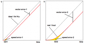
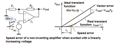
Jiri Dostal drew attention to high-speed distortions back in 1981. This type of distortion occurs whenever the signal deviates from the sinusoid and manifests itself to one degree or another. The music signal is not a sine wave, therefore this type of distortion is the most harmful for amplifiers designed to amplify music signals.3) Why are you focussing so much on speed distortion outside the audio band and what exactly is speed distortion
Transient distortions are associated with the behavior of the group delay. The smaller the group delay and the more linear and longer the linear section with a smooth falloff at the end, the less transient distortions.4) What is your definition of transient distortion, because feeding a burst to a filter causes a change of shape, which is not the same as distortion.
Noise offset is precisely what occurs due to velocity distortion. The lower the signal propagation delay, the lower the noise floor in the audio range. You can verify this by reading the comparison test of the two amplifiers. Although at 20 kHz the loop gain in the Hafler amplifier is 2 dB higher than in the Hiraga amplifier, it nevertheless has a higher noise floor.5) What exactly is noise bias
Attachments
Cyril Hammer said well about the need for a low time propagayion delay
Cyril Hammer, The Absolute Sound_ May/June 2012
https://www.moremusic.nl/reviews/passlabs/XP-30-TAS.pdf
“Perfect performance in the time domain is no less important. This is especially true of amplifiers
based on negative feedback. The theoretical concept of negative feedback is very powerful, and the
simplified mathematical equations describing this concept do hold true. But they are only valid if the design addresses the limitations of the concept. The time delay from input to output must be zero!
Obviously in real life this is not possible. There are two ways to deal with this problem. Either you just do not apply any negative feedback at all to your design (while giving up the advantages of the concept) or you do speed it up to the level (200 MHz in the case of the Soulution 700 and 710) of a few nanoseconds of time delay from input to output, where timing errors are so small that they do not have any audible impact on the sound. Once you decide to go the latter way a whole bunch of new challenges suddenly arise. Thermal conditions, stability of supply voltages, high-frequency designs, noise induction etc., etc.»
As for the noise stand. Compare tests of three amplifiers
http://forum.vegalab.ru/showthread.php?t=72049&p=2451108&viewfull=1#post2451108
http://forum.vegalab.ru/showthread.php?t=72049&p=2451108&viewfull=1#post2451108
Attachments
Hans, note the relationship between bias, distortion spectrum, and switching distortion.
compare with similar parameters of the EE2008-04 output stage
Musings on amp design... a thread split.
compare with similar parameters of the EE2008-04 output stage
Musings on amp design... a thread split.
Attachments
-
 OPS_Like_SAPR_Loop-Gain.png32.5 KB · Views: 76
 -
 OPS_Like_SAPR_IMD_19-20kHz.png33.9 KB · Views: 72
 -
 OPS_Like_SAPR_cros-dist_(bias-100mA).png31.5 KB · Views: 72
 -
 OPS_Like_SAPR_cros-dist_(bias-29mA).png32.4 KB · Views: 97
 -
 OPS_Like_SAPR_20kHz-spectr_(bias-100mA).png80.3 KB · Views: 123
 -
 OPS_Like_SAPR_20kHz-spectr_(bias-29mA).png89.5 KB · Views: 120
 -
 OPS_Like_SAPR_THD&Freq.png94.7 KB · Views: 83
Last edited:
- Home
- Amplifiers
- Solid State
- Musings on amp design... a thread split