Hello guys.
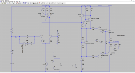
I'd like some feedback on the design in the attachments")
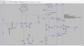
Basic idea is to get a "cost effective", reliable 20W per channel amplifier that works up to 2W in class A, then goes into class B. The initial name for it was "The Quick 'n Dirty" but it kinda grew. Thankfully it still has managable ammount of parts
The power devices will be MJW3281A + MJW1302A, drivers and VAS will be KSC3503 + KSA1381, other transistors are BC550C + BC560C.
I selected oversized output transistors hoping for reliability, but they also seem to be very linear devices judging from the datasheet.
Because of the quintescent current the idle dissipation will be around 20W per channel. I want to put both channels on the same extruded heatsink. I think that 0.7W/K should be good enough, giving around 25K temperature rise.
I don't know how big the transformer should be? Around 120VA?
Do you have any critiques of the schematic, or ideas of improvements? I added a strange way of current sinking the VAS - a JFET current source with bootstrapped feed point - simulation shows over 40 times less current fluctuation over just the CSS. Or is it better to go pure bootstrap for simplicity?
Another question is about the Vbe multiplier - what should be the current of the resistors vs the transistor? I went for around 10%.
The buffered VAS is almost literally lifted from "Designing Audio Power Amplifiers", along with the degenerated diff-pair.
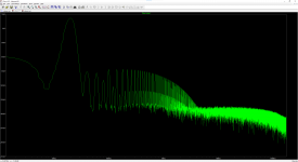
Distortion simulation:
I'd like some feedback on the design in the attachments
Basic idea is to get a "cost effective", reliable 20W per channel amplifier that works up to 2W in class A, then goes into class B. The initial name for it was "The Quick 'n Dirty" but it kinda grew. Thankfully it still has managable ammount of parts
The power devices will be MJW3281A + MJW1302A, drivers and VAS will be KSC3503 + KSA1381, other transistors are BC550C + BC560C.
I selected oversized output transistors hoping for reliability, but they also seem to be very linear devices judging from the datasheet.
Because of the quintescent current the idle dissipation will be around 20W per channel. I want to put both channels on the same extruded heatsink. I think that 0.7W/K should be good enough, giving around 25K temperature rise.
I don't know how big the transformer should be? Around 120VA?
Do you have any critiques of the schematic, or ideas of improvements? I added a strange way of current sinking the VAS - a JFET current source with bootstrapped feed point - simulation shows over 40 times less current fluctuation over just the CSS. Or is it better to go pure bootstrap for simplicity?
Another question is about the Vbe multiplier - what should be the current of the resistors vs the transistor? I went for around 10%.
The buffered VAS is almost literally lifted from "Designing Audio Power Amplifiers", along with the degenerated diff-pair.
Distortion simulation:
Is this any good? I know that the simulation uses different output transistors, but it should give some idea to more experienced designers than me.Simulated distortion at 2W:
1kHz:
Fourier components of V(fb)
DC component:-0.00829615
Harmonic Frequency Fourier Normalized Phase Normalized
Number [Hz] Component Component [degree] Phase [deg]
1 1.000e+03 5.713e+00 1.000e+00 -0.04° 0.00°
2 2.000e+03 1.337e-05 2.340e-06 179.01° 179.05°
3 3.000e+03 1.229e-05 2.151e-06 125.77° 125.82°
4 4.000e+03 6.356e-06 1.113e-06 -174.36° -174.32°
5 5.000e+03 5.522e-06 9.666e-07 -163.92° -163.88°
6 6.000e+03 4.061e-06 7.108e-07 -171.09° -171.05°
7 7.000e+03 3.348e-06 5.860e-07 -169.00° -168.96°
8 8.000e+03 2.848e-06 4.985e-07 -168.37° -168.33°
9 9.000e+03 2.431e-06 4.256e-07 -166.52° -166.48°
Total Harmonic Distortion: 0.000368%(0.010447%)
20kHz:
Fourier components of V(fb)
DC component:-0.00047394
Harmonic Frequency Fourier Normalized Phase Normalized
Number [Hz] Component Component [degree] Phase [deg]
1 2.000e+04 5.710e+00 1.000e+00 -2.64° 0.00°
2 4.000e+04 5.607e-06 9.820e-07 -171.99° -169.35°
3 6.000e+04 1.547e-04 2.709e-05 89.22° 91.86°
4 8.000e+04 2.673e-06 4.681e-07 -82.28° -79.64°
5 1.000e+05 6.515e-06 1.141e-06 -104.59° -101.95°
6 1.200e+05 2.596e-06 4.547e-07 -83.36° -80.72°
7 1.400e+05 3.294e-06 5.768e-07 -82.14° -79.50°
8 1.600e+05 2.590e-06 4.536e-07 -80.86° -78.22°
9 1.800e+05 2.546e-06 4.459e-07 -79.49° -76.85°
Total Harmonic Distortion: 0.002715%(0.014649%)
Simulated distortion at 20W:
1kHz:
Fourier components of V(fb)
DC component:-0.0261355
Harmonic Frequency Fourier Normalized Phase Normalized
Number [Hz] Component Component [degree] Phase [deg]
1 1.000e+03 1.802e+01 1.000e+00 -0.04° 0.00°
2 2.000e+03 4.731e-05 2.626e-06 162.42° 162.46°
3 3.000e+03 1.734e-04 9.622e-06 77.29° 77.33°
4 4.000e+03 2.033e-05 1.128e-06 -169.34° -169.30°
5 5.000e+03 7.043e-05 3.909e-06 82.99° 83.03°
6 6.000e+03 1.312e-05 7.281e-07 -169.73° -169.69°
7 7.000e+03 3.008e-05 1.670e-06 98.53° 98.57°
8 8.000e+03 9.625e-06 5.342e-07 -167.02° -166.98°
9 9.000e+03 1.468e-05 8.147e-07 156.30° 156.34°
Total Harmonic Distortion: 0.001097%(0.014298%)
20kHz:
Fourier components of V(fb)
DC component:-0.00146531
Harmonic Frequency Fourier Normalized Phase Normalized
Number [Hz] Component Component [degree] Phase [deg]
1 2.000e+04 1.801e+01 1.000e+00 -2.65° 0.00°
2 4.000e+04 7.307e-05 4.058e-06 168.82° 171.48°
3 6.000e+04 9.948e-04 5.525e-05 70.31° 72.96°
4 8.000e+04 1.388e-05 7.709e-07 2.20° 4.85°
5 1.000e+05 3.045e-04 1.691e-05 13.13° 15.78°
6 1.200e+05 8.406e-06 4.668e-07 -93.06° -90.41°
7 1.400e+05 2.128e-04 1.182e-05 55.56° 58.21°
8 1.600e+05 7.834e-06 4.351e-07 -69.22° -66.56°
9 1.800e+05 1.633e-04 9.066e-06 64.24° 66.90°
Total Harmonic Distortion: 0.005981%(0.015468%)
Attachments
Id say you've got a pretty good result there, though with only 47pF of compensation you may find it unstable in practice.
Consider using an LED for the LTP's current source reference. They are lower noise.
Also do a startup simulation using the options "startup uic" in LTSPICE. This will show you what the circuit will do on power up. Set the signal input to 0V when doing that
Consider using an LED for the LTP's current source reference. They are lower noise.
Also do a startup simulation using the options "startup uic" in LTSPICE. This will show you what the circuit will do on power up. Set the signal input to 0V when doing that
@jaycee About the LED vs Zener LTP reference - I started with a green LED in that position but then remembered that zener noise goes lower with accumulated on time. But that might have been about ovenized voltage references Also the output impedance of the CSS should be higher with higher reference voltage. I will go back to the LED though - seems a lot of amplifiers use them here.
Thanks for the comment about the miller cap - I read some more and found that Baxendall proposed to split the compensation at low frequency with a resistor from the midpoint of two capacitors in series in the position of the current miller cap to the amplifier output to get higher open loop gain - how would one pick optimal values?
On startup simulation I get a transient on the output towards the positive rail that settles to 0V after ~0.5ms, pushes 2.7A current spike into the load in this time.
No cross conduction in the output.
The VAS CSS doesn't go to full operating current for ~100ms - probably because of the bootstrap capacitor charging slowly - boostrap point takes ~2.5s to settle to its nornal operating voltage.
After VAS CSS loads the stage output gets biased.
Seems like 'normal' behaviour - would get a loud pop from the speaker likely.
Also the output impedance of the CSS should be higher with higher reference voltage. I will go back to the LED though - seems a lot of amplifiers use them here.Thanks for the comment about the miller cap - I read some more and found that Baxendall proposed to split the compensation at low frequency with a resistor from the midpoint of two capacitors in series in the position of the current miller cap to the amplifier output to get higher open loop gain - how would one pick optimal values?
On startup simulation I get a transient on the output towards the positive rail that settles to 0V after ~0.5ms, pushes 2.7A current spike into the load in this time.
No cross conduction in the output.
The VAS CSS doesn't go to full operating current for ~100ms - probably because of the bootstrap capacitor charging slowly - boostrap point takes ~2.5s to settle to its nornal operating voltage.
After VAS CSS loads the stage output gets biased.
Seems like 'normal' behaviour - would get a loud pop from the speaker likely.
Plan B, go for a 2.7-3 V zener, these are much quieter as well (thermal stability obviously is not quite as good).Consider using an LED for the LTP's current source reference. They are lower noise.
Input tail current of >2 mA seems a bit hot to me, I'd shoot for more like 1 mA. Slightly modify the VAS if need be.
If you do need 378 mA of idle current, 0R1 emitter resistors actually aren't optimum. Try something like 0R033 instead.
Use the edit button. Works for up to half an hour.Also is it possible to edit posts? I made a typo above
At least where it's important. The whole idea behind higher-order compensation is gaining higher open-loop gain in the audible and near ultrasonic range where it's needed, and then dropping back down quickly and returning to a first-order response before unity gain rolls around so that stability is not affected.Going back to TMC - more open loop gain should help distortion across the board, right?
That said, get the rest of the circuit sorted out first.
@kokoriantz Well class G and H are interesting, but complexity just goes up in exponential fashion
I'd go to class D for better efficiency, but 40 watts of idle power are not that bad for audio (At work we have triodes with around 500W of HEATER dissipation ;-) the thing is not for audio, but a HF generator with few kW of output power )
The whole aim of this project is to build a simple, but good linear amplifier, I can live with higher dissipation and a pricier heatsink And if the thing will work nice with lower quiescent current then I might go to more conservative biasing, higher rail voltages and just get 50W or more out of it anyway
But most importantly I want to design my own PCBs to improve my skills in the field.
@sgrossklass thanks for the pointer about lower voltage zener
About the LTP current - at lower current the transistors will get more hfe? Or what other motivation do we get here to lower the tail current? As is VAS + miller feedback needs ~71uA RMS drive current for 20W output power. Seems that lowering drive capability might hurt slew rate and THD?
The idle current was just somewhat random, I didn't play around much with it - probably 250mA might be enough for what I wanted to do. With emitter resistors you aim for some maximum voltage drop rule of thumb?
I edited the schematic a bit and thrown in TMC - at first glance it flattened out THD across the power range!!!
I'd go to class D for better efficiency, but 40 watts of idle power are not that bad for audio
(At work we have triodes with around 500W of HEATER dissipation ;-) the thing is not for audio, but a HF generator with few kW of output power )The whole aim of this project is to build a simple, but good linear amplifier, I can live with higher dissipation and a pricier heatsink
And if the thing will work nice with lower quiescent current then I might go to more conservative biasing, higher rail voltages and just get 50W or more out of it anyway But most importantly I want to design my own PCBs to improve my skills in the field.
@sgrossklass thanks for the pointer about lower voltage zener
About the LTP current - at lower current the transistors will get more hfe? Or what other motivation do we get here to lower the tail current? As is VAS + miller feedback needs ~71uA RMS drive current for 20W output power. Seems that lowering drive capability might hurt slew rate and THD?
The idle current was just somewhat random, I didn't play around much with it - probably 250mA might be enough for what I wanted to do. With emitter resistors you aim for some maximum voltage drop rule of thumb?
I edited the schematic a bit and thrown in TMC - at first glance it flattened out THD across the power range!!!
Last edited:
Design my own pcb's.
A power amp isnt a bad place to start but audio can be a minefield.
1/ Power supplies should be kept separate before the amplifier. Dont mix audio ground and smoothing caps ground or the charging impulses will modulate the ground line and you will get hum.
2/ Keep input traces short and preferable shielded where possible.
3/ Keep power tracks as thick as possible to cope with high currents.
4/ Star connect audio power ground and output zobel. Audio ground and other grounds should meet once at edge of pcb at power connector.
My first attempt at an audio pcb was a USB mixer.
I mixed in the audio and power supply grounds.
Result was with inputs shorted I was getting 1VRMS on output of hum !
Totally useless.
So looked up how to design a pcb,
Separated out power supply from mixer part and used a star ground.
Second pcb came back and was greatly improved.
Just connecting tracks together in the first place can be a challenge but doing what I suggest can be even more challenging. But well worth the effort.
Well I did some audio PCBs before, did some guitar effects, even managed to trace out a RIAA preamp that is dead silent - in the positive sense, ergo not broken ;-) Followed exact same advice you given here, had fair share of failures too
Just that this would be my first PA from start to finish ;-)
Just that this would be my first PA from start to finish ;-)
Last edited:
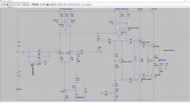
Okay, schematic after tweaks in attachments.
Changes:
Modified VAS miller feedback to TMC, lowered LTP tail current to ~1mA, lowered emitter resistances to 0R033, changed idle current to ~250mA.
Output offset increased, but is less than 0.5mV.
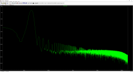
New distortion figures:
They seem very optimistic to me, LTSpice might be lying here?
EDIT: Simulation shows that on clipping negative excursions stick to the rail (bootstrap fault?) and positive have something that looks like gain inversion near waveform peak (horns on the waveform).
Changes:
Modified VAS miller feedback to TMC, lowered LTP tail current to ~1mA, lowered emitter resistances to 0R033, changed idle current to ~250mA.
Output offset increased, but is less than 0.5mV.
New distortion figures:
Code:
Simulated distortion at 2W:
1kHz:
Fourier components of V(fb)
DC component:-0.00866705

Harmonic	Frequency	 Fourier 	Normalized	 Phase  	Normalized
 Number 	  [Hz]   	Component	 Component	[degree]	Phase [deg]
    1   	1.000e+03	5.713e+00	1.000e+00	   -0.05°	    0.00°
    2   	2.000e+03	1.308e-05	2.289e-06	  176.92°	  176.97°
    3   	3.000e+03	7.567e-06	1.325e-06	 -176.65°	 -176.60°
    4   	4.000e+03	6.395e-06	1.119e-06	 -174.01°	 -173.96°
    5   	5.000e+03	4.991e-06	8.736e-07	 -173.34°	 -173.29°
    6   	6.000e+03	4.060e-06	7.108e-07	 -171.56°	 -171.51°
    7   	7.000e+03	3.361e-06	5.884e-07	 -169.78°	 -169.73°
    8   	8.000e+03	2.822e-06	4.940e-07	 -167.58°	 -167.54°
    9   	9.000e+03	2.435e-06	4.262e-07	 -166.65°	 -166.60°
Total Harmonic Distortion: 0.000321%(0.010275%)

20kHz:
Fourier components of V(fb)
DC component:-0.000845273

Harmonic	Frequency	 Fourier 	Normalized	 Phase  	Normalized
 Number 	  [Hz]   	Component	 Component	[degree]	Phase [deg]
    1   	2.000e+04	5.708e+00	1.000e+00	   -2.77°	    0.00°
    2   	4.000e+04	4.107e-06	7.195e-07	 -135.01°	 -132.24°
    3   	6.000e+04	1.362e-06	2.387e-07	 -121.11°	 -118.33°
    4   	8.000e+04	3.839e-06	6.726e-07	  -81.43°	  -78.66°
    5   	1.000e+05	3.078e-06	5.392e-07	  -79.82°	  -77.05°
    6   	1.200e+05	3.829e-06	6.709e-07	  -77.37°	  -74.59°
    7   	1.400e+05	3.678e-06	6.443e-07	  -76.47°	  -73.70°
    8   	1.600e+05	3.851e-06	6.748e-07	  -72.95°	  -70.17°
    9   	1.800e+05	3.804e-06	6.664e-07	  -70.88°	  -68.11°
Total Harmonic Distortion: 0.000176%(0.009541%)


Simulated distortion at 20W:
1kHz:
Fourier components of V(fb)
DC component:-0.0265072

Harmonic	Frequency	 Fourier 	Normalized	 Phase  	Normalized
 Number 	  [Hz]   	Component	 Component	[degree]	Phase [deg]
    1   	1.000e+03	1.802e+01	1.000e+00	   -0.05°	    0.00°
    2   	2.000e+03	4.358e-05	2.419e-06	  161.17°	  161.22°
    3   	3.000e+03	4.893e-06	2.716e-07	 -164.84°	 -164.79°
    4   	4.000e+03	2.057e-05	1.142e-06	 -169.87°	 -169.82°
    5   	5.000e+03	1.495e-05	8.297e-07	 -170.13°	 -170.08°
    6   	6.000e+03	1.362e-05	7.559e-07	 -168.35°	 -168.30°
    7   	7.000e+03	1.098e-05	6.097e-07	 -166.95°	 -166.90°
    8   	8.000e+03	9.875e-06	5.481e-07	 -165.00°	 -164.96°
    9   	9.000e+03	8.545e-06	4.743e-07	 -163.98°	 -163.93°
Total Harmonic Distortion: 0.000306%(0.014295%)

20kHz:
Fourier components of V(fb)
DC component:-0.00183475

Harmonic	Frequency	 Fourier 	Normalized	 Phase  	Normalized
 Number 	  [Hz]   	Component	 Component	[degree]	Phase [deg]
    1   	2.000e+04	1.800e+01	1.000e+00	   -2.77°	    0.00°
    2   	4.000e+04	3.866e-05	2.148e-06	  179.35°	  182.13°
    3   	6.000e+04	4.826e-05	2.681e-06	  -18.77°	  -16.00°
    4   	8.000e+04	1.001e-05	5.561e-07	  -55.73°	  -52.96°
    5   	1.000e+05	1.400e-04	7.780e-06	    7.01°	    9.78°
    6   	1.200e+05	1.023e-05	5.682e-07	  -88.09°	  -85.32°
    7   	1.400e+05	1.472e-04	8.177e-06	    5.06°	    7.83°
    8   	1.600e+05	9.171e-06	5.095e-07	  -79.04°	  -76.26°
    9   	1.800e+05	1.554e-04	8.633e-06	    5.39°	    8.16°
Total Harmonic Distortion: 0.001465%(0.014481%)EDIT: Simulation shows that on clipping negative excursions stick to the rail (bootstrap fault?) and positive have something that looks like gain inversion near waveform peak (horns on the waveform).
Attachments
Last edited:
At this lower idle current, go to 0R039 or 0R047.Changes:
Modified VAS miller feedback to TMC, lowered LTP tail current to ~1mA, lowered emitter resistances to 0R033, changed idle current to ~250mA.
Yes and no.They seem very optimistic to me, LTSpice might be lying here?
Yes - perfectly matched parts at constant equal temperature, perfect impedance balance, and I think BJT parasitic capacitance nonlinearity still is not modeled particularly well, so things would definitely tend to be optimistic.
No - even as-is, you're hitting some accuracy / compression related limits, I think. I'd suggest adopting something like this:
Code:
.option plotwinsize 0
.param freq=1k
.param period=1/freq ncycles=15 startrec=0
.param validcycles=ncycles-startrec
.tran 0 {ncycles*period} {startrec*period} {pi/3.14*period/2e3}
.four {freq} 19 {validcycles-1} V(out-amp)A "blameless" 80 wpc amp can hit <0.001% THD, so results of this magnitude definitely are quite feasible.
You should probably go research the subject of clamping diodes and other rail sticking fixes.EDIT: Simulation shows that on clipping negative excursions stick to the rail (bootstrap fault?) and positive have something that looks like gain inversion near waveform peak (horns on the waveform).
BTW - output inductor? (~1.5 µH || 4R7 or so)
Last edited:
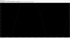
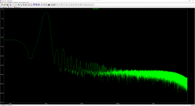
I added the inductor (it is parallel with 4R7, it just isn't visible in the schematic) and simulated the circuit again, FFT plots, actual schematic and asc in attachments. (Haven't touched the rail sticking problem yet.)
I changed SPICE relative tolerance to 1E-12 to get more accurate simulation (should I go even lower?).
1kHz 2W:
20kHz 2W:
1kHz 20W:
20kHz 20W:
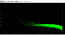
Seems that .fourier is not accurate (20kHz @ 2W has almost 0 THD... while in the plots it has clearly more than 1kHz @ 2W).
Also there are large ammounts of high order odd harmonics for 20kHz @ 20W - how can I fix this? Miller comp?
offtopic: can I make the code tags to collapse?
I changed SPICE relative tolerance to 1E-12 to get more accurate simulation (should I go even lower?).
1kHz 2W:
Code:
Circuit: * C:\Users\jimra\Documents\LTspiceXVII\qdpamp.asc

Direct Newton iteration failed to find .op point.  (Use ".option noopiter" to skip.)
Starting Gmin stepping
Gmin = 10
Gmin = 1.07374
Gmin = 0.115292
Gmin = 0.0123794
Gmin = 0.00132923
Gmin = 0.000142725
Gmin = 1.5325e-005
Gmin = 1.6455e-006
Gmin = 1.76685e-007
Gmin = 1.89714e-008
Gmin = 2.03704e-009
Gmin = 2.18725e-010
Gmin = 2.34854e-011
Gmin = 2.52173e-012
Gmin = 2.70769e-013
Gmin = 0
Gmin stepping succeeded in finding the operating point.

Heightened Def Con from 1.08745e-007 to 2.59074e-006
N-Period=14
Fourier components of V(out-amp)
DC component:-0.00880021

Harmonic	Frequency	 Fourier 	Normalized	 Phase  	Normalized
 Number 	  [Hz]   	Component	 Component	[degree]	Phase [deg]
    1   	1.000e+03	5.719e+00	1.000e+00	   -0.12°	    0.00°
    2   	2.000e+03	1.348e-05	2.357e-06	  174.42°	  174.54°
    3   	3.000e+03	7.407e-06	1.295e-06	  179.14°	  179.26°
    4   	4.000e+03	6.714e-06	1.174e-06	 -179.66°	 -179.54°
    5   	5.000e+03	5.601e-06	9.794e-07	  179.78°	  179.89°
    6   	6.000e+03	4.464e-06	7.806e-07	 -179.94°	 -179.83°
    7   	7.000e+03	3.671e-06	6.419e-07	 -179.81°	 -179.69°
    8   	8.000e+03	3.346e-06	5.850e-07	 -179.99°	 -179.88°
    9   	9.000e+03	3.096e-06	5.413e-07	  179.76°	  179.88°
   10   	1.000e+04	2.677e-06	4.682e-07	  179.97°	  180.08°
   11   	1.100e+04	2.340e-06	4.092e-07	 -179.80°	 -179.69°
   12   	1.200e+04	2.230e-06	3.899e-07	 -179.97°	 -179.85°
   13   	1.300e+04	2.116e-06	3.700e-07	  179.96°	  180.08°
   14   	1.400e+04	1.913e-06	3.345e-07	 -179.97°	 -179.85°
   15   	1.500e+04	1.789e-06	3.129e-07	  179.96°	  180.07°
   16   	1.600e+04	1.672e-06	2.924e-07	  179.99°	  180.10°
   17   	1.700e+04	1.508e-06	2.637e-07	 -179.70°	 -179.59°
   18   	1.800e+04	1.489e-06	2.604e-07	 -179.96°	 -179.85°
   19   	1.900e+04	1.501e-06	2.625e-07	  179.45°	  179.57°
Total Harmonic Distortion: 0.000352%(0.007735%)


Date: Mon Jan 11 13:39:44 2021
Total elapsed time: 22.094 seconds.

tnom = 27
temp = 27
method = modified trap
totiter = 787846
traniter = 787018
tranpoints = 263999
accept = 263942
rejected = 58
matrix size = 85
fillins = 98
solver = Alternate
Matrix Compiler1: 15.74 KB object code size  3.1/2.5/[2.3]
Matrix Compiler2: 10.85 KB object code size  1.6/2.7/[1.4]
20kHz 2W:
Code:
Circuit: * C:\Users\jimra\Documents\LTspiceXVII\qdpamp.asc

Direct Newton iteration failed to find .op point.  (Use ".option noopiter" to skip.)
Starting Gmin stepping
Gmin = 10
Gmin = 1.07374
Gmin = 0.115292
Gmin = 0.0123794
Gmin = 0.00132923
Gmin = 0.000142725
Gmin = 1.5325e-005
Gmin = 1.6455e-006
Gmin = 1.76685e-007
Gmin = 1.89714e-008
Gmin = 2.03704e-009
Gmin = 2.18725e-010
Gmin = 2.34854e-011
Gmin = 2.52173e-012
Gmin = 2.70769e-013
Gmin = 0
Gmin stepping succeeded in finding the operating point.

Heightened Def Con from 4.48844e-008 to 2.66488e-006
N-Period=14
Fourier components of V(out-amp)
DC component:-0.000843717

Harmonic	Frequency	 Fourier 	Normalized	 Phase  	Normalized
 Number 	  [Hz]   	Component	 Component	[degree]	Phase [deg]
    1   	2.000e+04	5.707e+00	1.000e+00	   -4.12°	    0.00°
    2   	4.000e+04	3.301e-06	5.785e-07	  160.05°	  164.16°
    3   	6.000e+04	1.253e-06	2.195e-07	   81.44°	   85.56°
    4   	8.000e+04	2.488e-08	4.360e-09	    3.01°	    7.12°
    5   	1.000e+05	5.878e-07	1.030e-07	  104.99°	  109.10°
    6   	1.200e+05	1.248e-08	2.187e-09	 -173.40°	 -169.28°
    7   	1.400e+05	4.049e-08	7.095e-09	   -9.62°	   -5.50°
    8   	1.600e+05	9.582e-09	1.679e-09	 -179.08°	 -174.96°
    9   	1.800e+05	9.387e-08	1.645e-08	  123.49°	  127.60°
   10   	2.000e+05	7.065e-09	1.238e-09	  178.82°	  182.93°
   11   	2.200e+05	5.443e-08	9.537e-09	 -105.22°	 -101.10°
   12   	2.400e+05	6.502e-09	1.139e-09	  171.25°	  175.37°
   13   	2.600e+05	3.164e-08	5.544e-09	   80.49°	   84.60°
   14   	2.800e+05	6.108e-09	1.070e-09	 -171.04°	 -166.92°
   15   	3.000e+05	3.453e-09	6.051e-10	 -125.68°	 -121.56°
   16   	3.200e+05	4.148e-09	7.268e-10	  171.98°	  176.10°
   17   	3.400e+05	4.010e-08	7.027e-09	 -136.69°	 -132.57°
   18   	3.600e+05	4.177e-09	7.319e-10	 -164.30°	 -160.18°
   19   	3.800e+05	5.247e-08	9.194e-09	   31.16°	   35.28°
Total Harmonic Distortion: 0.000063%(0.000000%)


Date: Mon Jan 11 13:37:52 2021
Total elapsed time: 23.776 seconds.

tnom = 27
temp = 27
method = modified trap
totiter = 855381
traniter = 854553
tranpoints = 284318
accept = 283808
rejected = 511
matrix size = 85
fillins = 98
solver = Alternate
Matrix Compiler1: 15.74 KB object code size  3.1/2.4/[2.3]
Matrix Compiler2: 10.85 KB object code size  1.5/1.8/[1.4]
1kHz 20W:
Code:
Circuit: * C:\Users\jimra\Documents\LTspiceXVII\qdpamp.asc

Direct Newton iteration failed to find .op point.  (Use ".option noopiter" to skip.)
Starting Gmin stepping
Gmin = 10
Gmin = 1.07374
Gmin = 0.115292
Gmin = 0.0123794
Gmin = 0.00132923
Gmin = 0.000142725
Gmin = 1.5325e-005
Gmin = 1.6455e-006
Gmin = 1.76685e-007
Gmin = 1.89714e-008
Gmin = 2.03704e-009
Gmin = 2.18725e-010
Gmin = 2.34854e-011
Gmin = 2.52173e-012
Gmin = 2.70769e-013
Gmin = 0
Gmin stepping succeeded in finding the operating point.

Heightened Def Con from 4.74233e-008 to 2.58742e-006
N-Period=14
Fourier components of V(out-amp)
DC component:-0.0270889

Harmonic	Frequency	 Fourier 	Normalized	 Phase  	Normalized
 Number 	  [Hz]   	Component	 Component	[degree]	Phase [deg]
    1   	1.000e+03	1.815e+01	1.000e+00	   -0.12°	    0.00°
    2   	2.000e+03	4.571e-05	2.519e-06	  157.70°	  157.81°
    3   	3.000e+03	4.349e-06	2.397e-07	  161.38°	  161.49°
    4   	4.000e+03	2.118e-05	1.167e-06	 -177.83°	 -177.71°
    5   	5.000e+03	1.570e-05	8.650e-07	  179.00°	  179.11°
    6   	6.000e+03	1.420e-05	7.824e-07	  179.83°	  179.95°
    7   	7.000e+03	1.156e-05	6.370e-07	  179.74°	  179.86°
    8   	8.000e+03	1.065e-05	5.870e-07	  179.94°	  180.06°
    9   	9.000e+03	9.371e-06	5.164e-07	  178.90°	  179.01°
   10   	1.000e+04	8.521e-06	4.695e-07	  179.98°	  180.09°
   11   	1.100e+04	7.743e-06	4.267e-07	  179.59°	  179.71°
   12   	1.200e+04	7.095e-06	3.910e-07	  180.00°	  180.11°
   13   	1.300e+04	6.506e-06	3.585e-07	  179.41°	  179.52°
   14   	1.400e+04	6.076e-06	3.348e-07	 -179.99°	 -179.87°
   15   	1.500e+04	5.682e-06	3.131e-07	  179.76°	  179.87°
   16   	1.600e+04	5.314e-06	2.928e-07	 -179.97°	 -179.85°
   17   	1.700e+04	5.085e-06	2.802e-07	  179.86°	  179.97°
   18   	1.800e+04	4.724e-06	2.603e-07	  179.99°	  180.10°
   19   	1.900e+04	4.444e-06	2.449e-07	  179.87°	  179.98°
Total Harmonic Distortion: 0.000337%(0.007969%)


Date: Mon Jan 11 13:31:11 2021
Total elapsed time: 22.777 seconds.

tnom = 27
temp = 27
method = modified trap
totiter = 813376
traniter = 812548
tranpoints = 271224
accept = 271134
rejected = 91
matrix size = 85
fillins = 98
solver = Alternate
Matrix Compiler1: 15.74 KB object code size  3.1/3.2/[2.3]
Matrix Compiler2: 10.85 KB object code size  1.5/1.8/[1.4]
20kHz 20W:
Code:
Circuit: * C:\Users\jimra\Documents\LTspiceXVII\qdpamp.asc

Direct Newton iteration failed to find .op point.  (Use ".option noopiter" to skip.)
Starting Gmin stepping
Gmin = 10
Gmin = 1.07374
Gmin = 0.115292
Gmin = 0.0123794
Gmin = 0.00132923
Gmin = 0.000142725
Gmin = 1.5325e-005
Gmin = 1.6455e-006
Gmin = 1.76685e-007
Gmin = 1.89714e-008
Gmin = 2.03704e-009
Gmin = 2.18725e-010
Gmin = 2.34854e-011
Gmin = 2.52173e-012
Gmin = 2.70769e-013
Gmin = 0
Gmin stepping succeeded in finding the operating point.

Heightened Def Con from 2.57666e-008 to 2.66477e-006
Heightened Def Con from 0.000224917 to 0.000226064
Heightened Def Con from 0.000374968 to 0.000376067
Heightened Def Con from 0.000474887 to 0.000476068
Heightened Def Con from 0.000574933 to 0.000576069
Heightened Def Con from 0.000674914 to 0.000676069
N-Period=14
Fourier components of V(out-amp)
DC component:-0.00184026

Harmonic	Frequency	 Fourier 	Normalized	 Phase  	Normalized
 Number 	  [Hz]   	Component	 Component	[degree]	Phase [deg]
    1   	2.000e+04	1.811e+01	1.000e+00	   -4.12°	    0.00°
    2   	4.000e+04	4.058e-05	2.241e-06	  161.67°	  165.79°
    3   	6.000e+04	2.926e-05	1.616e-06	  -50.20°	  -46.08°
    4   	8.000e+04	4.962e-06	2.740e-07	   -0.03°	    4.09°
    5   	1.000e+05	6.752e-05	3.728e-06	   -0.90°	    3.22°
    6   	1.200e+05	1.573e-06	8.688e-08	 -141.22°	 -137.10°
    7   	1.400e+05	6.801e-05	3.755e-06	   -6.74°	   -2.62°
    8   	1.600e+05	4.647e-07	2.566e-08	 -121.05°	 -116.93°
    9   	1.800e+05	7.107e-05	3.925e-06	  -10.37°	   -6.25°
   10   	2.000e+05	7.458e-07	4.119e-08	 -142.31°	 -138.19°
   11   	2.200e+05	6.939e-05	3.832e-06	  -12.79°	   -8.67°
   12   	2.400e+05	6.333e-07	3.497e-08	 -146.95°	 -142.83°
   13   	2.600e+05	6.602e-05	3.646e-06	  -14.26°	  -10.14°
   14   	2.800e+05	6.030e-07	3.330e-08	 -153.56°	 -149.44°
   15   	3.000e+05	6.158e-05	3.401e-06	  -14.91°	  -10.79°
   16   	3.200e+05	5.531e-07	3.054e-08	 -158.55°	 -154.43°
   17   	3.400e+05	5.682e-05	3.138e-06	  -15.18°	  -11.06°
   18   	3.600e+05	5.022e-07	2.773e-08	 -163.36°	 -159.25°
   19   	3.800e+05	5.191e-05	2.867e-06	  -14.77°	  -10.65°
Total Harmonic Distortion: 0.001043%(0.000000%)


Date: Mon Jan 11 13:35:21 2021
Total elapsed time: 32.714 seconds.

tnom = 27
temp = 27
method = modified trap
totiter = 1191702
traniter = 1190874
tranpoints = 389544
accept = 387853
rejected = 1697
matrix size = 85
fillins = 98
solver = Alternate
Matrix Compiler1: 15.74 KB object code size  3.1/2.5/[2.3]
Matrix Compiler2: 10.85 KB object code size  1.6/1.8/[1.4]
Seems that .fourier is not accurate (20kHz @ 2W has almost 0 THD... while in the plots it has clearly more than 1kHz @ 2W).
Also there are large ammounts of high order odd harmonics for 20kHz @ 20W - how can I fix this? Miller comp?
offtopic: can I make the code tags to collapse?
Attachments
Last edited:
For a.c. R28 and R14 are in series. You are asking the feedback line to represent 0 volts in one sense and to drive R14 and modulate a constant current arrangement in another. The voltage drop across R14 would generate a feedback signal which would merge with that in R28. The only way that I can see to separate these paths is to connect R28 to ground.
For a.c. R28 and R14 are in series. You are asking the feedback line to represent 0 volts in one sense and to drive R14 and modulate a constant current arrangement in another. The voltage drop across R14 would generate a feedback signal which would merge with that in R28. The only way that I can see to separate these paths is to connect R28 to ground.
But FB is driven by low impedance output pair - so shouldn't this work as desired with R14 being bootstrapped through C8?
Then R28+C7 provides miller feedback from the output stage untill C10 impedance isn't smaller than R28 resistance (~500kHz), at which point miller feedback is closed just around the VAS with C7+C10 - this is how I see the arangement working here. Should give more open loop gain in acoustic frequencies than just straight miller compensation.
Last edited:
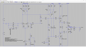
I think that I have arrived at the final version of the schematic.
I recalculated the emitter resistors for ~10:1 degeneration in all stages.
I replaced VAS transistors with TO92 packaged ones (BC5** series) due to low dissipation and Ccbo being just 2.5pF.
I modified the miller feedback a little, but this compensation scheme is somewhat black art to me But it seems to help higher frequency THD figures. Fortunately it's super simple to ommit if it will misbehave.
I was contemplating cascoding the VAS transistor, but decided it overkill and not contributing much for the added complexity.
The bootstrapped CSS can also be simply changed into a straight bootstrap or CSS for testing.
The driver was also modified to use CFPs instead of straight EFs - I wanted to unload the VAS, but didn't want 6VBE drops of the tripple topology. Without base stoppers at the output pair I got oscillation - seems to happen often with CFP. I might add the possibility to tame the lower pair with a small miller cap, but in the simulation base stoppers, well... stopped the oscillations. Also C1 (discharge cappacitor for the buffer) was moved away from the transistor bases, in front of the stoppers - in that position it amplified the oscillations(?).
I decided to use 346.7mA idle current and selected 0R075 emitter resistors for the output pair - might be cheaper to implement as controlled geometry tracks on the PCB than buying resistors of this value <= scratch that, this would need a 1mil trace of ~3.5mm length, no way it would survive the currents needed ;-)
Sugestions welcome as always
I have one question though - the output inductor shouldn't be in the global NFB loop, right?
I recalculated the emitter resistors for ~10:1 degeneration in all stages.
I replaced VAS transistors with TO92 packaged ones (BC5** series) due to low dissipation and Ccbo being just 2.5pF.
I modified the miller feedback a little, but this compensation scheme is somewhat black art to me
But it seems to help higher frequency THD figures. Fortunately it's super simple to ommit if it will misbehave.I was contemplating cascoding the VAS transistor, but decided it overkill and not contributing much for the added complexity.
The bootstrapped CSS can also be simply changed into a straight bootstrap or CSS for testing.
The driver was also modified to use CFPs instead of straight EFs - I wanted to unload the VAS, but didn't want 6VBE drops of the tripple topology. Without base stoppers at the output pair I got oscillation - seems to happen often with CFP. I might add the possibility to tame the lower pair with a small miller cap, but in the simulation base stoppers, well... stopped the oscillations. Also C1 (discharge cappacitor for the buffer) was moved away from the transistor bases, in front of the stoppers - in that position it amplified the oscillations(?).
I decided to use 346.7mA idle current and selected 0R075 emitter resistors for the output pair - might be cheaper to implement as controlled geometry tracks on the PCB than buying resistors of this value
<= scratch that, this would need a 1mil trace of ~3.5mm length, no way it would survive the currents needed ;-)Sugestions welcome as always
I have one question though - the output inductor shouldn't be in the global NFB loop, right?
Attachments
Last edited:
I think if one was to draw up a Gm plot of the output stage Ic on the x axis and Vbe on the y axis the angle of the plot would be very steep and with near to 350 m.A. of standing current.
As the result the crossover point would be at an intermediate power level. If one is going to cross over water make that a stream rather than a river getting up near flood levels.
I hope you are just using MJE transistors for simulation purposes. You need something beefier than 150XX types.
As the result the crossover point would be at an intermediate power level. If one is going to cross over water make that a stream rather than a river getting up near flood levels.
I hope you are just using MJE transistors for simulation purposes. You need something beefier than 150XX types.
- Status
- This old topic is closed. If you want to reopen this topic, contact a moderator using the "Report Post" button.
- Home
- Amplifiers
- Solid State
- Need feedback on DIY AB power amplifier