Hello gents (ladies?), I was hoping to get a bit of feedback on the amplifier design I've been working on, as in an amplifier design you can't have too much feedback, right? But before I arrive at what sort of feedback I'm looking for exactly please allow me to provide some background about the design.
As I was looking to busy myself during lockdown I revisited some of my earlier designs, some dating back well over a decade. This particular design initially started out as a rather elaborate exercise with lots and lots of transistors utilized to build cascodes and a plethora of precision current sources and mirrors. Then I realized that there's beauty in simplicity and elegance, so I started reducing it to something a bit more rudementary, which led me to where I'm currently at.
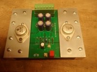
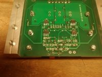
Upon looking at the schematic anyone that has ever dabbled with amplifier design will see the familiar three stage approach, but with optimizations left and right, let me briefly go over them to illustrate why I arrived at them:
1) The classic LTP input stage has a Wilson current mirror and features a pickoff point for the ETMC (Edmond Stuart) compensation I'm using (C12 and R37). The Wilson current mirror provided noticeable benefits over the standard current mirror, for the cost of an extra two transistors, so I figured that was worth it.
2) The current source feeding the input pair is the regular two transistor variety, nothing fancy here, I tried elaborate schemes, but those didn't seem to provide any benefit, but willing to try again if needed.
3) The VAS, to be honest I prefer to use the more correct term TIS, is your typical contraption, Q19 and R38+R39 as well as C12 and R37 provide the ETMC compensation. Q7 is the typical EF transistor with R40 used to protect Q7 during clip. Q17 serves a similar purposes but during a shortciruit at the output. Q18 makes sure the TIS can adequately drive the output stage. The TMC compensation rounds off the TIS stage and hooks directly to the output stage.
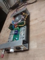
4) The output stage itself uses two pairs of Exicon lateral MOSFETs as that saves me a lot of headaches, and transistors, coming up with a foolproof protection if I had used a BJT output stage. They're biased a little beyond the point where their tempco becomes positive, which means they'll automagically provide temperature compensation. Due to the absence of a 2nd breakdown and the fact that lateral MOSFET's aren't a dead short when driven hard they have a wide SOA and I could get away with a simple protection mechanism.
Transistors Q15+Q16 and diodes D3+D4 take care of that, as they will reduce the drive voltage and limit the maximum current to about 8A per lateral MOSFET, which yields about 15A peak, more than enough for most loudspeakers.
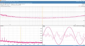
So, and this should really have been in the first paragraph, what are the requirements I set for the design of this amplifier? Well, a balanced input paired with simplicity and elegance is one, getting as close to the proverbial holy grail of -120dB/100W/8R/20kHz is another. With the current design the simulator optimistically reports 0.0003%, or rather -110dB, so quite close to target.
Closed loop gain shows ~88 degrees at the 0dB point, and the gain plot looks nice and smooth, as does the phase plot. That, in a nutshell, sums up the design. What I would love your input on is whether there's any elegant ways to further improve performance I might have missed?
Please find the relevant plots attached, as well as the LTspice .asc file for the amplifier design.
Thanks for applying feedback! I'm looking forward to applying your ideas and hopefully further improve on the design!
As I was looking to busy myself during lockdown I revisited some of my earlier designs, some dating back well over a decade. This particular design initially started out as a rather elaborate exercise with lots and lots of transistors utilized to build cascodes and a plethora of precision current sources and mirrors. Then I realized that there's beauty in simplicity and elegance, so I started reducing it to something a bit more rudementary, which led me to where I'm currently at.
Upon looking at the schematic anyone that has ever dabbled with amplifier design will see the familiar three stage approach, but with optimizations left and right, let me briefly go over them to illustrate why I arrived at them:
1) The classic LTP input stage has a Wilson current mirror and features a pickoff point for the ETMC (Edmond Stuart) compensation I'm using (C12 and R37). The Wilson current mirror provided noticeable benefits over the standard current mirror, for the cost of an extra two transistors, so I figured that was worth it.
2) The current source feeding the input pair is the regular two transistor variety, nothing fancy here, I tried elaborate schemes, but those didn't seem to provide any benefit, but willing to try again if needed.
3) The VAS, to be honest I prefer to use the more correct term TIS, is your typical contraption, Q19 and R38+R39 as well as C12 and R37 provide the ETMC compensation. Q7 is the typical EF transistor with R40 used to protect Q7 during clip. Q17 serves a similar purposes but during a shortciruit at the output. Q18 makes sure the TIS can adequately drive the output stage. The TMC compensation rounds off the TIS stage and hooks directly to the output stage.
4) The output stage itself uses two pairs of Exicon lateral MOSFETs as that saves me a lot of headaches, and transistors, coming up with a foolproof protection if I had used a BJT output stage. They're biased a little beyond the point where their tempco becomes positive, which means they'll automagically provide temperature compensation. Due to the absence of a 2nd breakdown and the fact that lateral MOSFET's aren't a dead short when driven hard they have a wide SOA and I could get away with a simple protection mechanism.
Transistors Q15+Q16 and diodes D3+D4 take care of that, as they will reduce the drive voltage and limit the maximum current to about 8A per lateral MOSFET, which yields about 15A peak, more than enough for most loudspeakers.
So, and this should really have been in the first paragraph, what are the requirements I set for the design of this amplifier? Well, a balanced input paired with simplicity and elegance is one, getting as close to the proverbial holy grail of -120dB/100W/8R/20kHz is another. With the current design the simulator optimistically reports 0.0003%, or rather -110dB, so quite close to target.
Closed loop gain shows ~88 degrees at the 0dB point, and the gain plot looks nice and smooth, as does the phase plot. That, in a nutshell, sums up the design. What I would love your input on is whether there's any elegant ways to further improve performance I might have missed?
Please find the relevant plots attached, as well as the LTspice .asc file for the amplifier design.
Thanks for applying feedback! I'm looking forward to applying your ideas and hopefully further improve on the design!
Attachments
Very nice amp, Sander.
Do you think that the two drivers are needed, given that gates of laterals are not very hungry?
Including a Vbe bias generator is unusual. How does the quiescent vary through the operating temperatures?
Elegant compensation, excellent current limiting, and high loop gain. Very low distortion, and nice profile.
Cheers,
Hugh
Last edited:
Very nice amp, Sander.
Do you think that the two drivers are needed, given that gates of laterals are not very hungry?
Including a Vbe bias generator is unusual. How does the quiescent vary through the operating temperatures?
Elegant compensation, excellent current limiting, and high loop gain. Very low distortion, and nice profile.
Cheers,
Hugh
Thanks Hugh!
The drivers reduce the THD by about 10dB, so their addition was well worth it in my opinion. They’re biased at 16mA to better be able to suck the (significant) gate charge out of the MOSFEts.
The bias generator is there to better control the temperature drift if you bias the lateral MOSFETs below the point where their tempco switches from positive to negative. In that case there’s significant drift in the heatsink temperature, the simple Vbe bias generator keeps that in check. The prototype will need to show whether this is a real world requirement, if not I’ll revert back to a simple trimpot.
Thanks Suzy!
Hugh suggested the same, please see my reply to him for an explanation why.
Hugh suggested the same, please see my reply to him for an explanation why.
Looks cool, but is Q16 a bias compensator? Laterals have negative temp coefficient, as you mentioned, so no need for that.
Sander,
Thanks for the answers....... helpful and instructive.
Of that 10dB reduction of THD was this 2-5 harmonics, or 5-20 harmonics? I ask because the Zout of the emitter followers is typically 26/12= 2R yet the stoppers are 47R and it seems to me that the impedance issue is secondary; it could be caused by the fast flow of charge into and out of the gate, and this could be achieved with highish current (18mA or so) between two collectors.
How did you arrive at the 47R stopper values? I have never seen definitive values given for the ECW lateral series..
I'm very much impressed with the THD, very low indeed.
Hugh
You want feedback, I like your new 6C33 avatar, they look like small Androids! ")
Ok, I have more like questions than any real feedback as I am maybe not 100 about all the fascinating intricate circuits in this amplifier.
First I am curious how the so called compensation network is supposed to work circulating around C12 R37, to my eyes it looks like it's adding positive feedback gain at higher frequencies, how or what exactly is it doing?
R40 on Q7 collector, isn't it possible to omit this resistor as it will degrade the BW and increase distortion through the non-linear miller C, if we want to protect Q7 from saturating and burning up, then perhaps a low Vf diode with anode to its base connected to Q8 collector would ensure that wont happen as when Q8 saturates it will pull Q7 base down.
Next, I am wondering if Q18 really is necessary as the lateral Op FET's have so low Crss and are already buffered with Q9 and Q10. A suggest modification could be to change Q8 for a smaller signal bjt and cascode it with ksa1381, although this isn't that necessary as Q8 is already buffered by Q7.
The current limit through output FET's set to 15A seems not the correct figure, maybe I am wrong but it looks rather like the double or even quadruple, that is because when one side of the OP stage is conducting, the other side is turned off, therefore there will be a voltage fall only over R24/25 or R26/27.
So if one assume there's roughly 0,7V per silicone device (1N4148 is actually lower, maybe closer to 0,5), in order for the Q15 and Q16 to activate we would need 0,7+0,7+0,5+0,5=2,4V, and 2,4V over each resistor pair (only the upper or lower pair) would yild 24A per R, or for a double 48A peak.
Oh, and a last one, some thoughts on Q6 Vbe multiplier, it may be too aggressive and pull back quiescent current too much, the laterals tempco goes neutral at around 100mA and negative above that, so what could be one viable option if we want to keep the Vbe multiplier is to leave Q6 stay put on the PCB instead of attached to the heat sink directly, that would make it react much gentler and only sensing the total ambient temperature adjusting less aggressively.
Although a simple R trimpot is actually enough with latfets.
Cheers Michael
Last edited:
Some yrs ago I got my hands on some original NOS 2SK135/2SJ50. This inpired me, after decades, to design an latFET-amp using extensively LTSpice. Out came a Monoblock with one pair of LatFETs intended as ultra-rigid lab ref amp with a bandwidth of several 100kHz. The technical data measured at the prototype are excellent and should be quite encouraging to build your own latFET amp.
Attachments
Of that 10dB reduction of THD was this 2-5 harmonics, or 5-20 harmonics? I ask because the Zout of the emitter followers is typically 26/12= 2R yet the stoppers are 47R and it seems to me that the impedance issue is secondary; it could be caused by the fast flow of charge into and out of the gate, and this could be achieved with highish current (18mA or so) between two collectors.
I see this reduction at 100W/8R/20kHz, I've not been looking at lower frequencies to be honest as my thinking was that those automatically will be significantly reduced as the loopgain is much higher at lower frequencies.
How did you arrive at the 47R stopper values? I have never seen definitive values given for the ECW lateral series.
These seem to work well with the optimized VDMOS (with treshold) models I used for the ECW series in the simulator. I'm going to take the pragmatic approach to optimizing them IRL though, simply by swapping out values and running successive THD measurements on the prototype. Bob Cordell used a different approach with RC networks on the gates, might give that a try too.
My thinking is that I can spend weeks in the simulator and never get a definitive answer whilst an afternoon spent on the workbench with a prototype will give me better results quicker.
I'm very much impressed with the THD, very low indeed.
Cheers, this was a careful balancing act with a lot of Monte Carlo scripting in LTspice to allow me to zero in on optimal component values. Luckily I don't have 40+ transistors in this design so this was somewhat manageable still.
If you replace Q6 to the KSC3503/KSA1381 pair wired as diodes you'll pick near ideal thermal tracking of the driver stage.
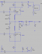
Thanks BesPav, that's very elegant indeed, thanks for the suggestion. See attached updated schematic.
By the way, you can pick much more feedback depth and a way higher unity-gain freq with such an output stage.
I would love to hear what suggestions you have for this!
Attachments
Hi Sander
I am glad Hugh pointed me into this thread.
You have some special solutions that I did not know of like the ETMC (Edmond Stuart) and the use of Q18 to help drive the output.
My suggestions are:
Use another bjt to serve as controller in the TIS CCS as Q5 and Q2 share the same Q1 and current variations in the TIS will modulate the CCS of the LTP.
Use a separated heatsink for the VBE multiplier not connected to the main heatsink.
I would increase C2 to maybe 330p and also R20 to 2k or more as IMO the TMC compensation although it provides splendid bass reproduction, can sometimes produce a too edgy trebble. I would also try a 10n cap between R20 and the Nfb node as like that you loose less OLG.
I am not really sure you need Q15 and Q16... I normally use diodes and zeners to limit the voltage swing in the lateral gates.
Why did you use two different transistors for Q1 and Q2 ?
The laterals gate resistors seem very low in value... if it oscilates you can try 15p caps between the gates and drains of the laterals.
How do you control output offset without using a dc blocking cap in the NFB circuit ?
Last edited:
You want feedback, I like your new 6C33 avatar, they look like small Androids!
Different topic but I actually designed a SE 6C33 amplifier using just tubes with very low distortion, see attached measurement plot.
First I am curious how the so called compensation network is supposed to work circulating around C12 R37, to my eyes it looks like it's adding positive feedback gain at higher frequencies, how or what exactly is it doing?
This is a compensation scheme developed by my fellow Dutchman Edmond Stuart (search the forum for ETMC) and basically injects some of the signal back into the TIS originating from the 180 degree out of phase signal at the LTP input pair.
R40 on Q7 collector, isn't it possible to omit this resistor as it will degrade the BW and increase distortion through the non-linear miller C, if we want to protect Q7 from saturating and burning up, then perhaps a low Vf diode with anode to its base connected to Q8 collector would ensure that wont happen as when Q8 saturates it will pull Q7 base down.
Yes and no, the resistor obviously prevents the EF transistor Q7 from burning to a crisp during clip (>5W dissipation), using a low Vf (and low capacitance) diode as you suggest is indeed a good trick. The downside is that it introduces a non-linear, voltage dependent, capacitance to the TIS, which results in a +20dB increase in distortion. The effect of the resistor R40 is far more benign and thus the lesser of two evils in this particular case.
Next, I am wondering if Q18 really is necessary as the lateral Op FET's have so low Crss and are already buffered with Q9 and Q10. A suggest modification could be to change Q8 for a smaller signal bjt and cascode it with ksa1381, although this isn't that necessary as Q8 is already buffered by Q7.
That was my first thought too, I've tried different approaches, including the (Hawksford) cascode, but the current configuration proved to give the highest overall loopgain without any peaking and thus the lowest distortion.
The current limit through output FET's set to 15A seems not the correct figure, maybe I am wrong but it looks rather like the double or even quadruple, that is because when one side of the OP stage is conducting, the other side is turned off, therefore there will be a voltage fall only over R24/25 or R26/27.
So if one assume there's roughly 0,7V per silicone device (1N4148 is actually lower, maybe closer to 0,5), in order for the Q15 and Q16 to activate we would need 0,7+0,7+0,5+0,5=2,4V, and 2,4V over each resistor pair (only the upper or lower pair) would yild 24A per R, or for a double 48A peak.
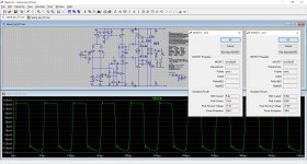
Well, I simulated this rather extensively, so unless I'm doing something wrong, or misinterpreting the results, that's what I'm seeing. Please have a look at the attached screenshot, this is the current delivered by Q13+Q14, about 8A peak, since I have two output pairs that adds up to 16A.
Oh, and a last one, some thoughts on Q6 Vbe multiplier, it may be too aggressive and pull back quiescent current too much, the laterals tempco goes neutral at around 100mA and negative above that, so what could be one viable option if we want to keep the Vbe multiplier is to leave Q6 stay put on the PCB instead of attached to the heat sink directly, that would make it react much gentler and only sensing the total ambient temperature adjusting less aggressively.
Although a simple R trimpot is actually enough with latfets.
Good suggestions, and similar to what others have suggested. BesPav's idea was the most elegant though; connecting the KSC3503 as a diode as due to its tempco it'll track the output stage tempco very neatly.
As for the bias current, I'm using the ECW20x20 lateral MOSFETs, these are double-die devices, hence they need about 200mA of quiescent current for entering the negative tempco zone.
Attachments
Some yrs ago I got my hands on some original NOS 2SK135/2SJ50. This inpired me, after decades, to design an latFET-amp using extensively LTSpice. Out came a Monoblock with one pair of LatFETs intended as ultra-rigid lab ref amp with a bandwidth of several 100kHz. The technical data measured at the prototype are excellent and should be quite encouraging to build your own latFET amp.
Very nice, thanks for sharing!
Use another bjt to serve as controller in the TIS CCS as Q5 and Q2 share the same Q1 and current variations in the TIS will modulate the CCS of the LTP.
I tried that, but that made the THD worse, I think the mechanism at play here is that modulation of the LTP current due to the TIS current helps with the ETMC compensation as they both are driven from the same LTP input pair.
Use a separated heatsink for the VBE multiplier not connected to the main heatsink.
As suggested by BesPav having Q6 connected as a diode and mounted on the main heatsink will track the output stage almost perfectly, as it'll see a positive tempco whereas the output stage sees a negative tempco.
I would increase C2 to maybe 330p and also R20 to 2k or more as IMO the TMC compensation although it provides splendid bass reproduction, can sometimes produce a too edgy trebble. I would also try a 10n cap between R20 and the Nfb node as like that you loose less OLG.
Noted! the values in have in the schematic are actually quite conservative already, I can go lower for C2, C3 and R20 and not suffer instability. Could you perhaps explain how inserting a 10n capacitor helps with preserving OLG as I'm drawing a blank and the simulator is not giving many clues either, I see similar loopgain with and without it.
I am not really sure you need Q15 and Q16... I normally use diodes and zeners to limit the voltage swing in the lateral gates.
The ECW20x20 lateral MOSFETs have built in 14V gate zeners, so I don't need additional zeners, how would you connect the diodes exactly? The reason Q15+Q16 are there is to prevent excessive dissipation in the MOSFETs when the output is shorted.
Why did you use two different transistors for Q1 and Q2 ?
Dissipation, Q2 dissipates about 200mW which is a bit on the high side for a TO92, especially when the PCB is mounted in a chassis as the ambient temperature will be >>25 degrees C.
The laterals gate resistors seem very low in value... if it oscilates you can try 15p caps between the gates and drains of the laterals.
Noted! I plan to evaluate the actual required stopper resistor values on the bench with a prototype, if they end up being too larger I'll indeed switch to using a C or and RC on the gate.
How do you control output offset without using a dc blocking cap in the NFB circuit ?
R7+R8 will be a trimpot, so I can set offset after the amplifier has warmed up, I'm seeing uVs in the simulator, if that turns out to be too optimistic and I see large (10s of mV) in practice I might opt for a DC servo.
Thanks for the suggestions!
One other option I evaluated was the use of Linear Systems LSJ689A P-channel JFETs for the input pair, see attached schematic, this works wonderfully in the simulator, with a 60% reduction in THD 20, but the moment I vary Idss of one of them by only 1% this input pair performs worse than the simple transistor variant, so I'm not sure whether that's wise. The other downside is the fact that the drain-source voltage is close to the rated maximum.
Linear Systems - LSJ689 dual P-channel JFET
http://www.linearsystems.com/lsdata...0 - LSJ689 Rev A9 dated 2019 07 23- Peter.pdf
Linear Systems - LSJ689 dual P-channel JFET
http://www.linearsystems.com/lsdata...0 - LSJ689 Rev A9 dated 2019 07 23- Peter.pdf
Attachments
Quote "Noted! the values in have in the schematic are actually quite conservative already, I can go lower for C2, C3 and R20 and not suffer instability. Could you perhaps explain how inserting a 10n capacitor helps with preserving OLG as I'm drawing a blank and the simulator is not giving many clues either, I see similar loopgain with and without it."
At low frequencies R20 dominates C2 and miller comp is dictated by C3. At low frequencies TMC loop gain will be smaller than miller loop gain by a factor of C2/(C3+C2)... if C3 = C2 this ratio is 0.5 and we will loose 6dB of global loop gain.
So C2 should be much larger than C3 (I normally use 10x)
In some cases the use of TMC produces a sharp increase in loop gain in the middle of the audio band. This peak can be eliminated by the inclusion of a 10n cap in series with R20.
Maybe you can not see any difference because you are using a very aggressive TMC.... try simulating the same with R20 = 10k.
Quote "The ECW20x20 lateral MOSFETs have built in 14V gate zeners, so I don't need additional zeners, how would you connect the diodes exactly? The reason Q15+Q16 are there is to prevent excessive dissipation in the MOSFETs when the output is shorted."
I was convinced these laterals did not have gate zeners that is why I included them in my builds.
I was convinced these laterals did not have gate zeners that is why I included them in my builds.
Attachments
I was convinced these laterals did not have gate zeners that is why I included them in my builds.
I contacted the manufacturer and they let me know the ECW20x20 lateral MOSFETs have 14V/1W zeners on die, it even states so in the datasheet, although somewhat cryptic, max. gate/source voltage +/-14V.
If I may make a suggestion? In your schematic I also see some MUR460 diodes, you don't need these either, as MOSFETs have an intrinsic body diode that's a result of the manufacturing process. These are well equipped to offer the overshoot protection you meant to implement with those diodes.
- Home
- Amplifiers
- Solid State
- Simplicity and elegance, feedback wanted!